Three Steps to Minimize Jitter in Gbps System Designs
The challenge of clock jitter—which adversely impacts high-speed protocols such as Ethernet, PCI Express®, and USB 3.0—is becoming more significant as next-generation protocols look to deliver data rates at hundreds of gigabits per second (Gbps). Understanding three key points can help you achieve success against jitter in your next design.
Timing is everything: which is why jitter skews everything up. Jitter noise on high-speed clocks degrades system performance, causing bit errors and limiting operating speed. The negative effects of jitter are proportional to voltage logic thresholds (noise margins) and to system operating frequencies. Characterized by the amount of deviation from ideal timing specified in picoseconds RMS, jitter is a major source of bit error rate (BER) degradation in high-frequency Gbps systems (see Figure 1). The BER is the percentage of bits with errors compared to total bits, so lower BER is always better.
This short article will:
- Describe how jitter affects data links at the receiver
- Explain the simplest way to reduce source jitter
- Show some examples of systems designed with low-jitter components
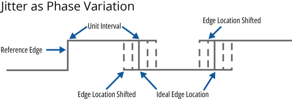
Figure 1: Jitter as the clock phase that is shifted from its expected position.
Point #1: High-performance data links require low jitter at receivers.
Jitter causes errors by shifting the sampling point away from the optimum time and into the region where the received bit is transitioning. This results in higher probability of getting the bit wrong.
The higher the data rate, the more sensitive the link is to jitter and the more precise the reference clock must be to achieve the desired performance goals. As data rates increase, jitter requirements tighten. Jitter in the reference clock will be amplified by PLLs in the system PHY or SERDES (see Figure 2), since these components respond to the clock edges.
The target BER for many common serial bus and expansion bus standards is 10-12
(1 bit error for every 1,000Gbits). The PCI Express 5.0 protocol, for example, specifies a clock jitter limit of 0.15ps RMS for 32.0GT/s (giga-transfers per second). By maintaining the system jitter below 0.15ps RMS, this BER of 10-12 is achieved.
The PI6CG33201C from Diodes Incorporated (Diodes) is an incredibly low-power PCIe clock generator, featuring a bench test PCIe max jitter of 0.05ps, thus offering a substantial margin against the PCIe 5.0 requirement of 0.15ps.
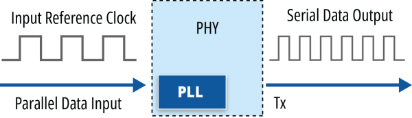
Figure 2: Jitter is amplified by clock timers and PLLs, compounding the problem.
Point #2: Start with a low-jitter clock source at the transmitter.
Since Gbps protocols such as HDMI (~ 10Gbps) or USB 3.0 (5Gbps) are highly sensitive to overall system clock jitter, it is critical to start with an “ultra-clean” (low-jitter) reference clock at the transmitter.
While jitter has many possible sources, the biggest “bang for buck” can be achieved through the source clock. A high-quality clock source widens the margin of the system jitter budget (“system” = source, Tx, link, Rx), reducing the need for extended and complex engineering efforts to reduce second- and third-order jitter sources like cross-coupled traces or inducted skin effects in PCBs.
How about in practice? Figure 3 shows a crystal oscillator demo board from Diodes with a 156.25MHz XO source. The latest small-size XO populated on this board is specified to have a maximum RMS jitter of <0.2ps, which is 30% lower than that required by 400G Interface, giving a comfortable Rx margin on an Ethernet link.
Using an Agilent phase noise analyzer, the XO exhibits a real-world jitter of 0.11ps, which is well below that required by 400GbE (Figure 4). This low-jitter clock source means that other components in the system can inject nearly 0.2ps additional jitter before the link jitter becomes out of spec (and out of an acceptable BER range). Clearly, starting with a low-jitter clock source gives a Gbps system designer more breathing room in a design.
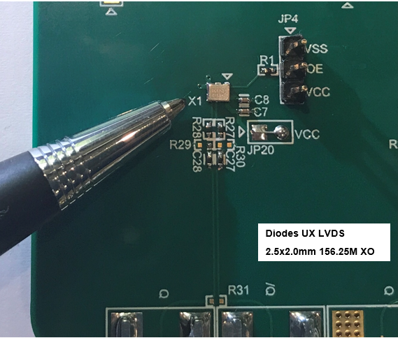
Figure 3: The UX 156.25MHz small-size XO demo board from Diodes is useful for demonstrating a low-jitter clock source. (Courtesy: Diodes Incorporated)
Point #3: Know how to use the XO in a system.
A typical Gbps system is shown in Figure 5. Here, an ultra-low-jitter XO feeds a clock buffer that provides multiple clocks for a variety of Gbps devices—including a 40GbE PHY, an Ethernet switch, and a ternary content addressable memory (TCAM), which is part of a layer 3 router. Diodes’ UX7 XO series is the heart of the low-jitter system and is capable of approximately 0.1ps (RMS) jitter, as measured between 12K – 20MHz and shown in Figure 4.
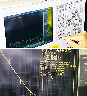
Figure 4: Using a phase noise analyzer by Agilent, the jitter of the demo board from Figure 3 is shown to be 0.111ps (seen as 111.949fs).
To avoid using multiple XOs in a system, the PI6C49S1510 clock buffer provides up to 10 output clocks (three are shown in Figure 5), with a very low additive jitter of 0.03ps. This essentially replicates the XO’s low jitter to all of the outputs. Figure 6 shows a screenshot of the same bench test as Figure 4 but at an output downstream of the clock buffer. Note that the total RMS jitter of the XO plus buffer is only 0.15ps RMS.
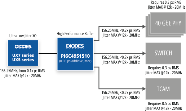
Figure 5: A typical low-jitter system starts with an ultra-low-jitter XO. (Courtesy: Diodes Incorporated)
For convenience, both the XO and the clock buffer run on 2.5VDC or 3.3VDC, further simplifying designs.
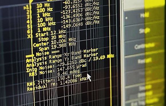
Figure 6: The total jitter of the notional system shown in Figure 5 using Diodes’ demo boards in the same bench set-up as Figure 4. Total additive jitter is a mere 0.15ps (RMS).
All-in-One XO and Buffer
Another way to create low-jitter systems besides what is depicted in Figure 5 is to use Diodes’ FlexOut clock generator, which combines an XO and clock buffer into a single package. The frequencies involved and the need for ultra-clean clocks are reasons the FlexOut PI6CXG06F62a offers an even lower jitter spec than the previously described XO (~0.1ps [typical]/0.15ps [max] from 12K – 20MHz) and supports up to six outputs in LVPECL and LVDS configurations.
The FlexOut’s main feature is that it requires no external XO. XO trace, terminations, and XO power filters are also not required. This device uses Diodes’ proprietary quartz timing source with a special clock IC, all miniaturized into a small LQFP package that is smaller than the two devices it replaces.
Regardless of which architecture a designer uses—XO alone, XO plus clock buffer, or an advanced combination device like the FlexOut—low BER Gbps systems require low jitter beginning at the transmitter, right at the clock source.
The Diodes logo is a registered trademark of Diodes Incorporated in the United States and other countries.
All other trademarks are the property of their respective owners.
© 2023 Diodes Incorporated. All Rights Reserved