Self-Protecting MOSFETs Deliver Improved Reliability in the Harsh Environment of Automotive Applications
Author: Ian Moulding, Automotive Marketing Manager
While it’s been said many times before, the automotive electrical environment is tough! As demonstrated in figure 1, the nominal battery voltage of an automobile can vary from -12V DC, under reverse battery condition, to +125V DC due to load transients and inductive field decay. Factor in wide variations in operating temperature, numerous interconnections and an open environment that is subject to possible ESD damage from human interactions, and you have an operating environment that is far more challenging than, for example, that of the consumer market segment.
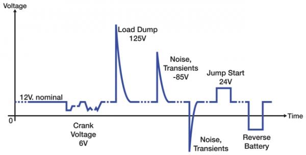
Figure 1. Causes of automotive battery voltage variations.
The automotive industry demands cost-effective and fully reliable solutions but this potentially destructive environment poses a huge challenge to the power semiconductor devices needed for the myriad of control functions that are now commonplace in modern automobiles.
Power semiconductors such as standard MOSFETs have been proven to be insufficiently rugged for many automotive applications. Inductive spikes and load dumps are transients that require either larger MOSFETs or external clamps to absorb the energy that would otherwise destroy the MOSFET. Both of these options add to the cost and complexity of discrete designs.
Self-protected MOSFETs, as developed by Diodes Incorporated, address this issue with monolithic circuit topologies that incorporate clamping and other protection features to provide a more reliable and lower cost/smaller size solution for driving relays, LEDs and other inductive loads.
Relay Driving
The DMN61D8LQ from Diodes Incorporated is a clamped-topology, self -protected MOSFET packaged in SOT-23 that has been optimized to meet the cost and performance needs of driving automotive relays. It features ESD protection on the input and active-drain clamping across the output. The latter is particularly useful when switching relays because, due to their inductive nature, large transients can be created when deactivating the relay and these transients have the potential to destroy unprotected MOSFETS.
The back-to-back Zener stack, shown in figure 2, between the MOSFET’s gate and drain connections, is the key component in this low-side, active clamp configuration. The clamp voltage is set by the Zener stack voltage and is designed to be less than the avalanche breakdown voltage of the MOSFET’s drain to source junction but high enough not to be triggered in normal operation.

Figure 2. Equivalent circuit of a low-side active over-voltage clamp.
This means that when the MOSFET is switched off, i.e. the input to the device is grounded, and the voltage of the drain pin rises above the Zener stack voltage, current will flow via the Zener and input resistor to ground. Then, as the resulting voltage generated at the gate of the MOSFET nears its threshold, the MOSFET will start to turn on and draw load current.
This ensures that the inductive energy generated by a deactivating relay is absorbed by the power MOSFET operating in its normal active region rather than dissipating the energy more locally in a reverse avalanche mode. And, since the clamp voltage is lower than the avalanche voltage, the MOSFET dissipates less instantaneous power in clamp mode than avalanche mode providing a greater energy handling capability.
Lamp Driving
To help cope further with transients, self-protected MOSFETs, such as the ZXMS6004FFQ from Diodes Incorporated, utilize a fully protected topology that incorporates over-temperature and over-current protection circuits. As can be seen in the block diagram in figure 3, this is in addition to an over-voltage and ESD input protection. This device leads the industry by using a small form factor SOT-23 package, 6x smaller than comparable SOT223-packaged parts.

Figure 3. The self-protection features of Diodes’ ZXMS6004FFQ MOSFET.
This self-protected MOSFET uses a temperature sensor and thermal shutdown circuit to protect against over-temperature. This circuit is active when the MOSFET is on and is triggered once a threshold temperature, typically 175°C, is exceeded. This turns off the MOSFET, interrupting the current flow to limit further heat dissipation. In-built hysteresis allows the output to automatically turn back on once the device has cooled by around 10°C.
An incandescent lamp has a low resistance when off, which rapidly increases when the lamp is switched on and heats up. Over-current protection, effected with a current limit circuit, not only protects against fault conditions but also avoids the high in-rush current associated with the lamp’s low turn-on resistance. The current limit circuit detects the substantial increase in MOSFET drain-source voltage (VDS) resulting from an excessive load current and reacts by reducing the internal gate drive and restricting the drain current (ID). This functionality protects the MOSFET and prolongs the life of the lamp and its behavior is illustrated in figure 4.

Figure 4. Typical output characteristic showing current limit function.
While these protection circuits are implemented independently they nevertheless normally function in combination. For example, over-current regulation can operate for some time but may not prevent the temperature eventually reaching the threshold where over-temperature cycling will kick in.
With their built-in protection features, self-protected MOSFETs provide a cost effective solution for switching loads in a wide variety of automotive applications. Their intrinsic features increase system reliability while the small size of the SOT-23 packaged devices from Diodes Incorporated offers significant space and cost-savings when compared to competitive devices.