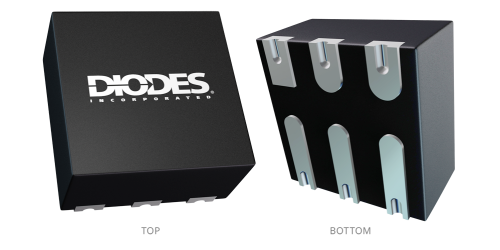
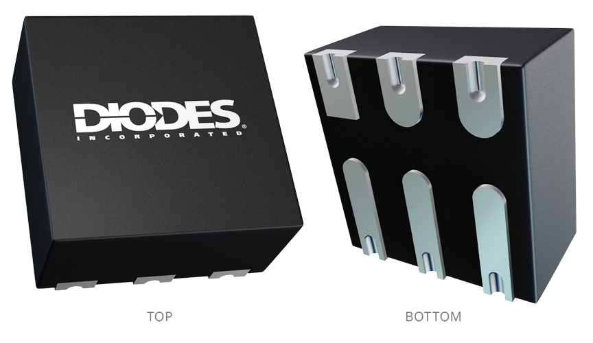
Image shown is for reference only. Actual package may vary. Refer to the product data sheet for package details. V-DFN1515-6/SWP (Type UX)
2.3V to 5.5V Input, 4A Synchronous Buck Converter
Log in or register to manage email notifications about changes to datasheets or PCNs for this part.
The AP61402 is a selectable up to 4A, synchronous buck converter with an input voltage range of 2.3V to 5.5V and fully integrates a 75mΩ high-side power MOSFET and a 33mΩ low-side power MOSFET to provide high-efficiency step-down DC/DC conversion.
The AP61402 is easily used by minimizing the external component count due to its adoption of constant on-time (COT) control to achieve fast transient responses, easy loop stabilization, and low output voltage ripple.
The AP61402 has optimized designs for small form factor. The series offers various fixed output voltage and an adjustable output voltage version. It also has a proprietary gate driver scheme to resist switching node ringing without sacrificing MOSFET turn-on and turn-off times, which reduces high frequency radiated EMI noise caused by MOSFET switching.
The device is available in a V-DFN1515-6/SWP (Type UX) package.
Compliance (Only Automotive Supports PPAP) |
Standard |
|---|---|
Type |
Buck |
HS RDS(ON) (mΩ) |
75 |
LS RDS(ON) (mΩ) |
33 |
MaximumInput Voltage (V) |
5.5 |
MinimumInput Voltage (V) |
2.3 |
Quiescent Current Typ (μA) |
20 |
Shutdown Current Typ (µA) |
0.03 |
Output Current (A) |
4 A |
Minimum Output Voltage (V) |
0.5 |
Maximum Output Voltage (V) |
5.5 |
Frequency Typ (kHz) |
2000 |
Features |
Enable Light Load Efficiency EN pin to set up PFM or Force PWM Power-Good Output Discharge Soft-start, Undervoltage Lockout (UVLO), VIN Overvoltage Protection (OVP), Thermal Shutdown |
Something went wrong with your request. Please try again later. If this problem continues, please contact Diodes support for assistance.
A PCN may only apply to specific orderable part numbers in this datasheet. Please refer to the corresponding PCN to see the exact orderable part number(s) affected.
| PCN # | Issue Date | Implementation Date | Subject |
|---|---|---|---|
| PCN-2770 | 2025-10-30 | 2025-10-30 | Add Fab Site Code, Country of Diffusion (COD) and Assembly Site Origin (ASO) on Product and Shipping Labels for all Diodes Products |
