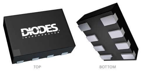
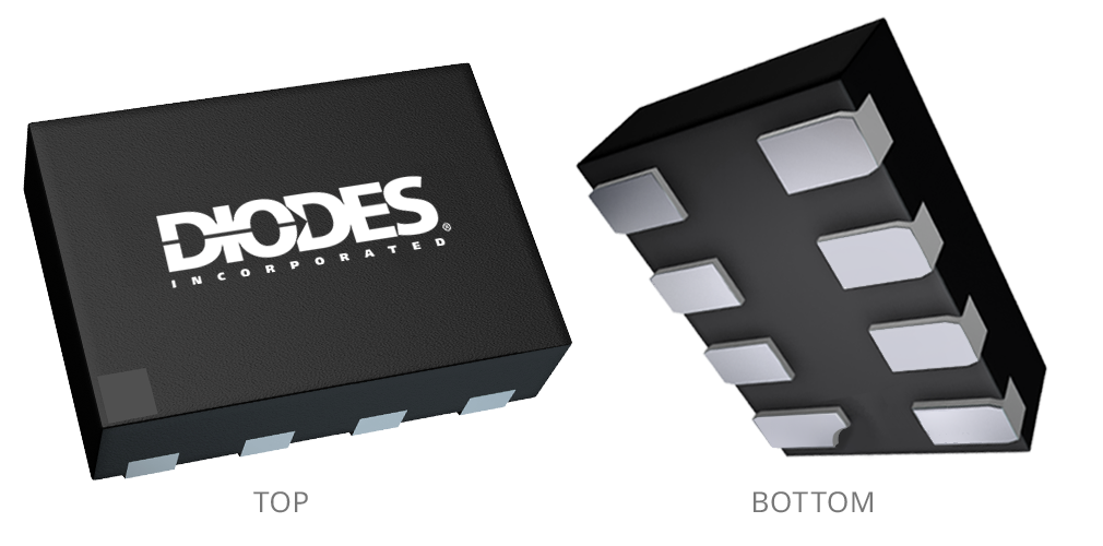
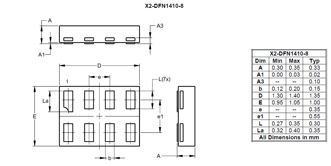
Image shown is for reference only. Actual package may vary. Refer to the product data sheet for package details. X1DFN (HK8) MSL1
Dual Bi-Directional I2C-bus and SMBus Voltage-Level Translator
Log in or register to manage email notifications about changes to datasheets or PCNs for this part.
The PI6ULS5V9306 is a dual bidirectional I2C-bus and SMBus voltage-level translator with an enable (EN) input. It is operational from 0.9V to 3.3V (VREF1) and 1.8V to 5V (VREF2).
The PI6ULS5V9306 allows bidirectional voltage translations between 1.0V and 5V without the use of a direction pin. The low ON-state resistance (Ron) of the switch allows connections to be made with minimal propagation delay. When EN is HIGH, the translator switch is on, and the SCL1 and SDA I/O are connected to the SCL2 and SDA2 I/O respectively, allowing bidirectional data flow between ports. When EN is LOW, the translator switch is off, and a high-impedance state exists between ports.
Compliance (Only Automotive Supports PPAP) |
Standard |
|---|---|
Translation From (V) |
1.2 to 3.3 |
Translation To (V) |
1.8 to 5 |
Max Signal Rate |
400kHz |
Bits Needed |
2 |
Auto Direction Sensing? |
Yes |
Shift |
Bi-Directional |
Ambient or Junction Temperature (°C) |
-40 to 85 |
Additional Technical Documents are available upon request:
Application information, Evaluation board, and Other technical documents
Something went wrong with your request. Please try again later. If this problem continues, please contact Diodes support for assistance.
A PCN may only apply to specific orderable part numbers in this datasheet. Please refer to the corresponding PCN to see the exact orderable part number(s) affected.
| PCN # | Issue Date | Implementation Date | Subject |
|---|---|---|---|
| PCN-2778 | 2025-12-01 | 2026-03-01 | Additional Wafer Source – (SPFAB) |
| PCN-2770 | 2025-10-30 | 2025-10-30 | Add Fab Site Code, Country of Diffusion (COD) and Assembly Site Origin (ASO) on Product and Shipping Labels for all Diodes Products |
| PCN-2723 | 2025-03-10 | 2025-09-10 | Product End of Life (EOL) |
| PCN-2654 | 2024-02-15 | 2024-04-28 | Device End of Life (EOL) |
| PCN-2602 | 2023-01-31 | 2023-07-31 | Device End of Life (EOL) |
| PCN-2510 | 2021-02-26 | 2021-05-26 | Qualified Additional A/T Sites, Fab Site and Data Sheet Change |
| PCN-2505 | 2021-01-26 | 2021-07-26 | Device End of Life (EOL) |
| PCN-2493 | 2020-12-28 | 2021-03-28 | Qualified Additional A/T Sites and Bill of Materials (BOM) |
