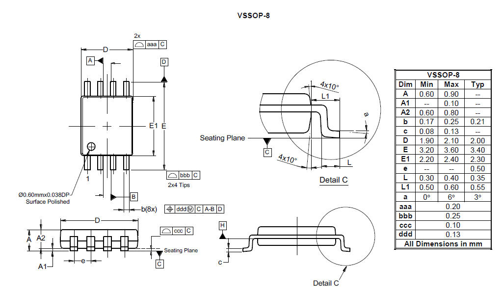
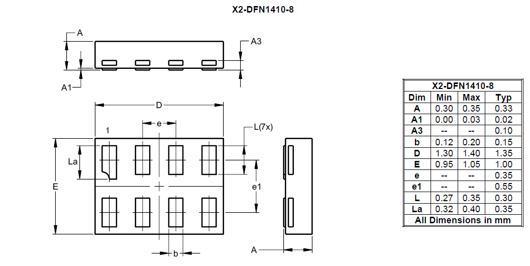
Image shown is for reference only. Actual package may vary. Refer to the product data sheet for package details. MSOP-8
2-Bits Bidirectional Level Translator, Open-Drain and Push-Pull Applications
Log in or register to manage email notifications about changes to datasheets or PCNs for this part.
The LSF0102 is a 2-channel bi-directional multi-voltage level translator for open-drain and push-pull applications. This device is a universal level translator that A port operates from 0.65V to 4.5V (Vref_A) and B port 1.8V to 5.5V (Vref_B). This range allows for bi-directional voltage translations between 0.65V and 5.0V. Be aware that Vref_B is recommended to be equal or higher than Vref_A for best signal integrity.
The EN pin is used to activate the device. When EN is HIGH, the translator switch is on. Otherwise, EN is LOW, the translator switch is off, and a high-impedance state exists between ports. The EN input circuit is designed to be supplied by Vref_B via an external Rpu (pullup resistor, typ 200kΩ) and the EN must be LOW during power-up or power-down to avoid miss operation.
Be aware that external Rpu (pullup resistor) is required on each signal in both A and B ports for push-pull application because a pull-high state can avoid miss operation during power-up or power-down. As same as open-drain application, the smaller Rpu results in the larger driving current. For bi-directional signal flows, there is no need for a direction pin to minimize system effort. This device supports 5V tolerant I/O pins in a variety of applications which require different voltage translation levels.
Compliance (Only Automotive Supports PPAP) |
Standard |
|---|---|
Translation From (V) |
0.65 to 4.5 |
Translation To (V) |
1.8 to 5.5 |
Max Signal Rate |
100MHz |
Bits Needed |
2 |
Auto Direction Sensing? |
No |
Shift |
Bi-Directional |
Prop Delay (ns) |
N/A |
Ambient or Junction Temperature (°C) |
-40 to 85 |
Additional Technical Documents are available upon request:
Application information, Evaluation board, and Other technical documents
Something went wrong with your request. Please try again later. If this problem continues, please contact Diodes support for assistance.
A PCN may only apply to specific orderable part numbers in this datasheet. Please refer to the corresponding PCN to see the exact orderable part number(s) affected.
| PCN # | Issue Date | Implementation Date | Subject |
|---|---|---|---|
| PCN-2778 | 2025-12-01 | 2026-03-01 | Additional Wafer Source – (SPFAB) |
| PCN-2770 | 2025-10-30 | 2025-10-30 | Add Fab Site Code, Country of Diffusion (COD) and Assembly Site Origin (ASO) on Product and Shipping Labels for all Diodes Products |
