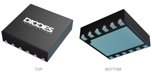
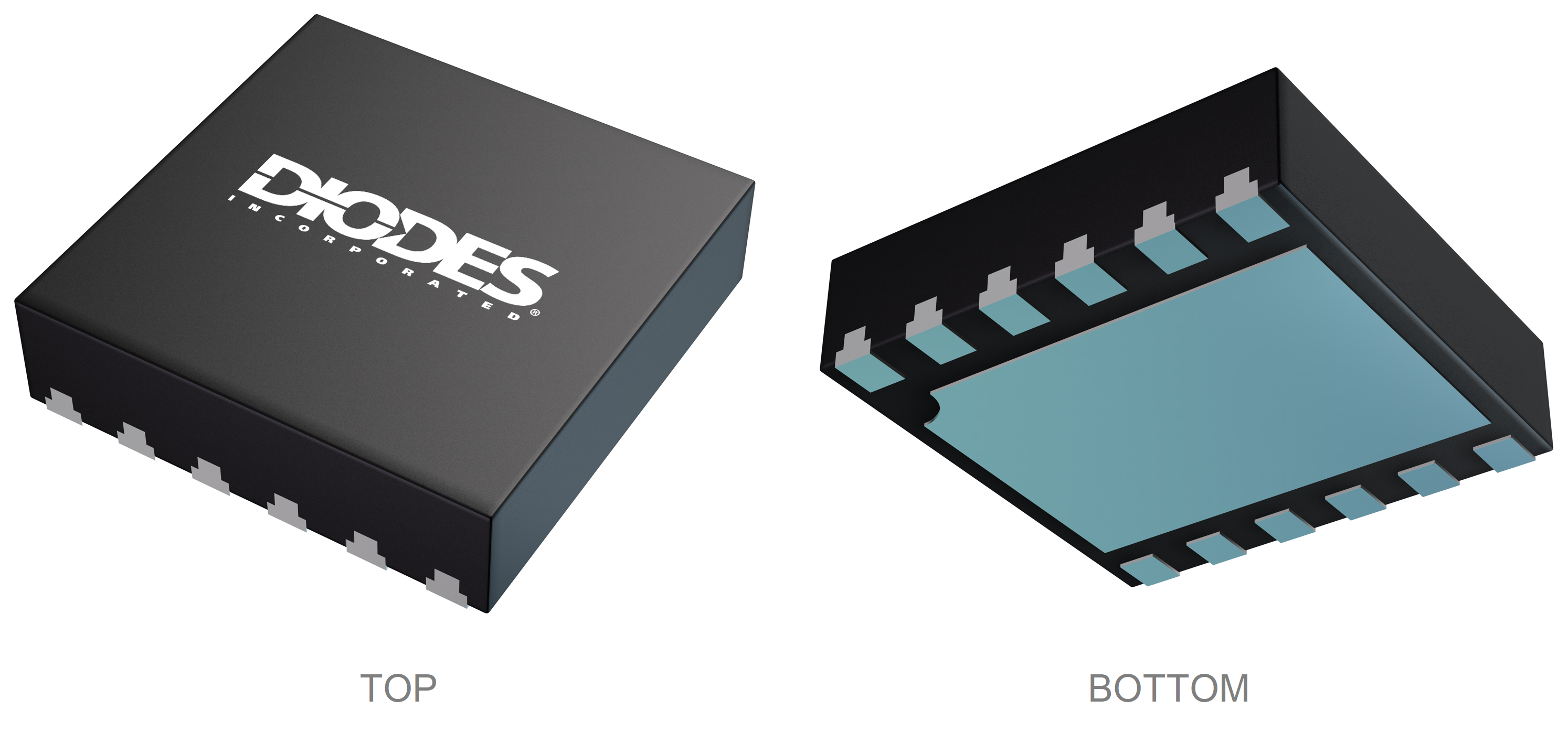
Image shown is for reference only. Actual package may vary. Refer to the product data sheet for package details. V-DFN3030-12 (Type B)
Single Channel Smart Load Switch
Log in or register to manage email notifications about changes to datasheets or PCNs for this part.
The DML3009LDC is a single channel load switch with very low onresistance in a small package. It contains an N-Channel MOSFET for up to 13.5V input voltage operation and 20A current channel. The load switch is controlled by a low voltage control signal through the ON Pin.
The DML3009LDC load switch provides a component and area-reducing solution for efficient power domain switching with inrush current limit via soft-start. In addition to integrated control functionality with ultra-low on-resistance, this device offers system safeguards and monitoring via fault protection and power good signaling. This cost-effective solution is ideal for power management and hot-swap applications requiring low-power consumption in a small footprint.
Type |
Load Switch |
|---|---|
AEC Qualified |
No |
Compliance (Only Automotive Supports PPAP) |
Standard |
Quiescent Current Typ (μA) |
310 |
Maximum Continuous Output Current (A) |
15 |
(MAX) Maximum Current Limit Fixed (A) |
Not Limited |
Adjustable Current Limit |
No |
Channels |
1 |
Enable Logic |
Active High |
Minimum Operating Voltage (V) |
0.5 |
Maximum Operating Voltage (V) |
13.5 |
RDS(ON) (VIN = 5V) Typ (mΩ) |
4.8 |
Reverse Current Block |
No |
Minimum Power Supply Voltage (V) |
3 |
Maximum Power Supply Voltage (V) |
5.5 |
Output Discharge |
Adjustable |
(TYP) Output Rise Time mS |
Adjustable |
OCP Output Latch Off |
No |
OCP/SCP |
SCP |
OCP Flag |
No |
Power Good |
open drain |
Overtemperature Protection |
Yes |
UL Certificate |
No |
Something went wrong with your request. Please try again later. If this problem continues, please contact Diodes support for assistance.
A PCN may only apply to specific orderable part numbers in this datasheet. Please refer to the corresponding PCN to see the exact orderable part number(s) affected.
| PCN # | Issue Date | Implementation Date | Subject |
|---|---|---|---|
| PCN-2770 | 2025-10-30 | 2025-10-30 | Add Fab Site Code, Country of Diffusion (COD) and Assembly Site Origin (ASO) on Product and Shipping Labels for all Diodes Products |
| PCN-2495 | 2021-03-31 | 2021-07-01 | Qualification of Additional Assembly & Test Sites and Additional Wafer Back Grinding and Back Metal Process Source for Select Discrete Products |
