Log in or register to manage email notifications about changes to datasheets or PCNs for this part.
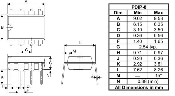
The AS358/358A consist of two independent, high gain and internally frequency compensated operational amplifiers, they are specifically designed to operate from a single power supply. Operation from split power supply is also possible and the low power supply current drain is independent of the magnitude of the power supply voltages. Typical applications include transducer amplifiers, DC gain blocks and most conventional operational amplifier circuits. The AS358/358A series are compatible with industry standard 358. AS358A has more stringent input offset voltage than AS358. The AS358 is available in SOIC-8, TSSOP-8 and MSOP-8 packages, AS358A is available in SOIC-8 package.
Compliance (Only Automotive Supports PPAP) |
Standard |
|---|---|
AEC Qualified |
No |
Number of Channels |
2 |
Minimum Supply Voltage (V) |
3 V |
Maximum Supply Voltage (V) |
36 V |
Supply Current @ 5V (per Op Amp) (mA) |
0.5 mA |
Input Offset Voltage typ (mV) |
2 mV |
Input Bias Current typ (nA) |
20 nA |
Minimum Input Common Mode Voltage (V) |
V- V |
Maximum Input Common Mode Voltage (V) |
V+ -1.5 V |
Output Current Source (mA) |
40 mA |
Output Current Sink (mA) |
15 mA |
Rail-Rail |
None |
Operating Ambient Temperature Range (°C) |
-40 to 85 °C |
Something went wrong with your request. Please try again later. If this problem continues, please contact Diodes support for assistance.
A PCN may only apply to specific orderable part numbers in this datasheet. Please refer to the corresponding PCN to see the exact orderable part number(s) affected.
| PCN # | Issue Date | Implementation Date | Subject |
|---|---|---|---|
| PCN-2770 | 2025-10-30 | 2025-10-30 | Add Fab Site Code, Country of Diffusion (COD) and Assembly Site Origin (ASO) on Product and Shipping Labels for all Diodes Products |
| PCN-2707 | 2024-12-30 | 2025-06-30 | Product End of Life (EOL) |
| PCN-2548 | 2021-10-08 | 2022-01-08 | Additional Wafer Source (JKFAB), New Bill of Materials (BOM) with PdCu Bond Wire, and Assembly/Test (A/T) Site (CAT) |
| PCN-2527 | 2021-06-09 | 2021-09-09 | Additional Wafer Source (GFAB, JKFAB), New Bill of Materials (BOM) with PdCu Bond Wire, and Additional Assembly/Test (A/T) Site (CAT) |
