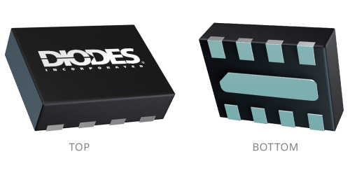
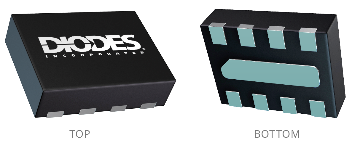
Image shown is for reference only. Actual package may vary. Refer to the product data sheet for package details. U-DFN2116-8
5V Single Channel Programmable Load Switch
Log in or register to manage email notifications about changes to datasheets or PCNs for this part.
Type |
Load Switch |
|---|---|
AEC Qualified |
No |
Compliance (Only Automotive Supports PPAP) |
Standard |
Quiescent Current Typ (μA) |
20 |
Maximum Continuous Output Current (A) |
4 |
(MAX) Maximum Current Limit Fixed (A) |
Not Limited |
Channels |
1 |
Enable Logic |
Active High |
Minimum Operating Voltage (V) |
1.5 |
Maximum Operating Voltage (V) |
5.5 |
RDS(ON) (VIN = 5V) Typ (mΩ) |
16 |
Reverse Current Block |
No |
Minimum Power Supply Voltage (V) |
1.5 |
Maximum Power Supply Voltage (V) |
5.5 |
Output Discharge |
Adjustable |
(TYP) Output Rise Time mS |
Adjustable |
OCP Flag |
No |
Power Good |
open drain |
Overtemperature Protection |
Yes |
UL Certificate |
No |
Something went wrong with your request. Please try again later. If this problem continues, please contact Diodes support for assistance.
A PCN may only apply to specific orderable part numbers in this datasheet. Please refer to the corresponding PCN to see the exact orderable part number(s) affected.
| PCN # | Issue Date | Implementation Date | Subject |
|---|---|---|---|
| PCN-2770 | 2025-10-30 | 2025-10-30 | Add Fab Site Code, Country of Diffusion (COD) and Assembly Site Origin (ASO) on Product and Shipping Labels for all Diodes Products |
| PCN-2554 | 2021-11-15 | 2022-02-15 | Qualified Additional Assembly & Test (A/T) Sites, Bill of Material (BOM) and updated Data Sheets for Package Outline Dimension Change |
