NRND = Not Recommended for New Design
HIGH-EFFICIENCY 1x/2x CHARGE PUMP FOR WHITE LED APPLICATIONS
Log in or register to manage email notifications about changes to datasheets or PCNs for this part.
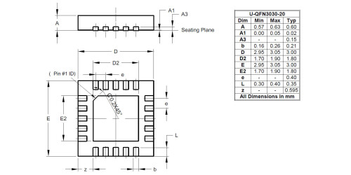
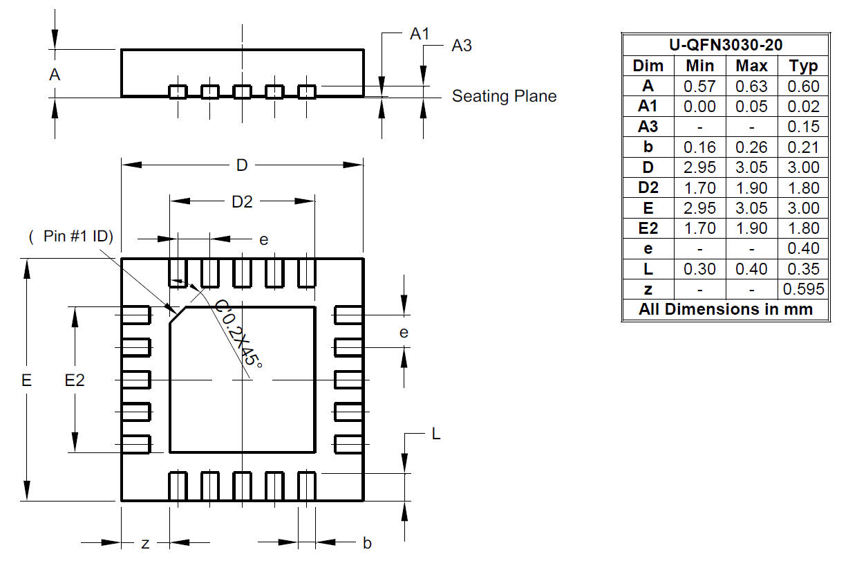
The AL3159 is a low noise, constant frequency charge pump DC/DC converter that uses a Dual mode load switch (1X), and (2X) conversion for white LED applications. The AL3159 is capable of driving nine LED channels at 20mA from a 2.7V to 5.5V input. The current sinks may be operated using three simple logic control inputs individually or in parallel for driving higher-current LEDs. Low external part counts (one 1µF flying capacitor and two 2.2µF capacitors at VIN and VOUT) make this part ideally suited for small, battery-powered applications. AL3159 digital inputs are used to enable or disable the LED channels with a fixed default current settings at 20mA. Each output of the AL3159 is equipped with built-in protection for VOUT short circuit and auto-disable for LED short conditions. Built-in soft-start circuitry prevents excessive inrush current during start-up and mode switching. A low-current shutdown feature disconnects the load from VIN to reduce quiescent current less than 1µA. The AL3159 is available in a lead-free, space-saving, thermally enhanced 20-pin 3 x 3mm QFN package.
AEC Qualified |
No |
|---|---|
AEC-Q100 Grade |
No |
Compliance (Only Automotive Supports PPAP) |
Standard |
Dimming |
PWM |
Dimming (Analog) |
No |
Dimming (PWM) |
No |
Efficiency (%) |
93 |
Efficiency (%) |
93 |
Function |
Charge Pump LED Driver |
LED Current (A) |
0.03 |
MaximumInput Voltage (V) |
5.5 |
Maximum LED Current (A) |
0.03 |
Maximum Output Current per Channel |
30 |
Maximum Output Voltage (V) |
5.5 |
Maximum Output Voltage (V) |
5.5 |
MinimumInput Voltage (V) |
2.7 |
Number of Regulated Output Channels |
9 |
OperatingTemperatureRange (°C) |
-40 to 85 |
Operating Temperature Range (°C) |
-40 to 85 |
OVP |
Yes |
AEC Qualified |
No |
Quiescent Current (µA) |
2 |
Quiescent Current Typ (μA) |
2 |
Quiescent Current Typ (mA) |
2 |
Soft Start |
Yes |
Standby Quiescent Current (µA) |
1 |
SW RDS(ON) |
0.5 |
Switching Frequency (MHz) |
1.2 |
Switching Frequency Maximum (kHz) |
1.2 |
Topologies (Boost) |
No |
Topologies (Buck-Boost) |
No |
Topologies (Buck) |
No |
Topologies (SEPIC) |
Yes |
Topology |
Charge Pump |
Typical Overcurrent Protection Current |
N/A |
VFB |
N/A |
Something went wrong with your request. Please try again later. If this problem continues, please contact Diodes support for assistance.
A PCN may only apply to specific orderable part numbers in this datasheet. Please refer to the corresponding PCN to see the exact orderable part number(s) affected.
| PCN # | Issue Date | Implementation Date | Subject |
|---|---|---|---|
| PCN-2770 | 2025-10-30 | 2025-10-30 | Add Fab Site Code, Country of Diffusion (COD) and Assembly Site Origin (ASO) on Product and Shipping Labels for all Diodes Products |
