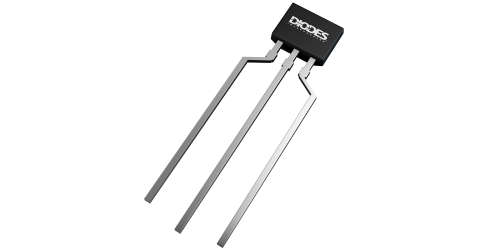
Image shown is for reference only. Actual package may vary. Refer to the product data sheet for package details. SIP-3 (Ammo)
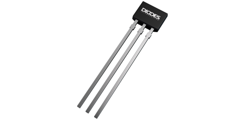
Image shown is for reference only. Actual package may vary. Refer to the product data sheet for package details. SIP-3 (Bulk)
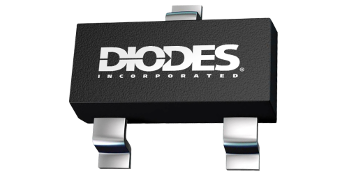
Image shown is for reference only. Actual package may vary. Refer to the product data sheet for package details. SOT23 (Type S)
High-Voltage High-Sensitivity Hall-Effect Latch With Internal Pullup Resistor
Log in or register to manage email notifications about changes to datasheets or PCNs for this part.
The AH3722A/AH3724A is a high-voltage, high-sensitivity Hall-effect latch IC with internal pullup resistor designed for commutation of brushless DC motors, flow meters, linear encoders and position sensors in industrial, consumer home appliances and personal care applications.
To support a wide range of the demanding applications, the design is optimized to operate over the supply range of 3.0V to 28V. With chopper stabilized architecture and an internal bandgap regulator to provide temperature compensated supply for internal circuits, the AH3722A/AH3724A provides a reliable solution over the whole operating range. For robustness and protection, the device has a Zener clamp on the supply. The output has an overcurrent limit and a Zener clamp.
The internally pulled-up output can be switched on with South pole of sufficient strength and switched off with North pole of sufficient strength. When the magnetic flux density (B) perpendicular to the part marking surface is larger than the operate point (BOP) the output is switched on (pulled low). The output is held latched until the magnetic flux density reverses and becomes lower than the release point (BRP).
Compliance (Only Automotive Supports PPAP) |
Standard |
|---|---|
Operating Ambient Temperature (°C) |
-40 to 125 |
AEC Qualified |
No |
Type |
Latch |
Outputs |
Single |
Output Type |
Pull-Up Resistor |
Active Output State (B > Bop) |
Low |
Inactive Output State (B < Brp) |
High |
Operating Voltage (V) |
3 to 28 |
Average Supply Current (mA) |
3 |
Min Operating Point Bop (Bops +ve/ Bopn -ve) (Gauss) |
10 |
Typ Operating Point Bop (Bops +ve/ Bopn -ve) (Gauss) |
25 |
Max Operating Point Bop (Bops +ve/ Bopn -ve) (Gauss) |
40 |
Min Release Point Brp (Brps +ve/ Brpn -ve) (Gauss) |
-40 |
Typ Release Point Brp (Brps +ve/ Brpn -ve) (Gauss) |
-25 |
Max Release Point Brp (Brps +ve/ Brpn -ve) (Gauss) |
-10 |
Output Current Capability (mA) |
30 |
Something went wrong with your request. Please try again later. If this problem continues, please contact Diodes support for assistance.
A PCN may only apply to specific orderable part numbers in this datasheet. Please refer to the corresponding PCN to see the exact orderable part number(s) affected.
| PCN # | Issue Date | Implementation Date | Subject |
|---|---|---|---|
| PCN-2770 | 2025-10-30 | 2025-10-30 | Add Fab Site Code, Country of Diffusion (COD) and Assembly Site Origin (ASO) on Product and Shipping Labels for all Diodes Products |
