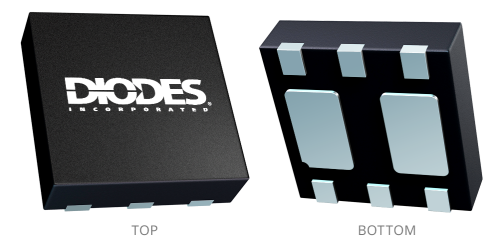
Image shown is for reference only. Actual package may vary. Refer to the product data sheet for package details. U-DFN2020-6 (Type B)
Complementary, 60V, 1A, DFN2020-6
Log in or register to manage email notifications about changes to datasheets or PCNs for this part.
Compliance (Only Automotive Supports PPAP) |
Standard |
|---|---|
Category |
Low Saturation Transistor |
Polarity |
NPN + PNP |
RCE(sat) (mΩ) |
240, 360 |
VCEO, VCES (V) |
60 |
IC (A) |
1 |
ICM (A) |
1.5 |
PD (W) |
1.6 |
hFE (Min) |
290, 170 |
hFE (@ IC) (A) |
0.1 |
hFE(Min 2) |
70 |
hFE (@ IC2) (A) |
1 |
VCE(sat) Max (mV) |
120, 180 |
VCE(SAT) (@ IC/IB) (A/mA) |
0.5/50 |
VCE(sat) (Max.2) (mV) |
240, 550 |
VCE(sat) (@ IC/IB2) (A/mA) |
1/50 |
fT (MHz) |
90, 65 |
Something went wrong with your request. Please try again later. If this problem continues, please contact Diodes support for assistance.
A PCN may only apply to specific orderable part numbers in this datasheet. Please refer to the corresponding PCN to see the exact orderable part number(s) affected.
| PCN # | Issue Date | Implementation Date | Subject |
|---|---|---|---|
| PCN-2770 | 2025-10-30 | 2025-10-30 | Add Fab Site Code, Country of Diffusion (COD) and Assembly Site Origin (ASO) on Product and Shipping Labels for all Diodes Products |
| PCN-2495 | 2021-03-31 | 2021-07-01 | Qualification of Additional Assembly & Test Sites and Additional Wafer Back Grinding and Back Metal Process Source for Select Discrete Products |
