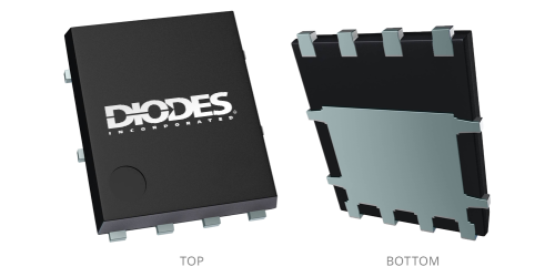
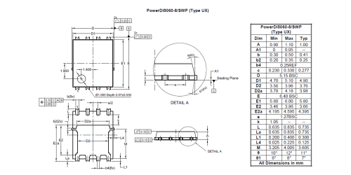
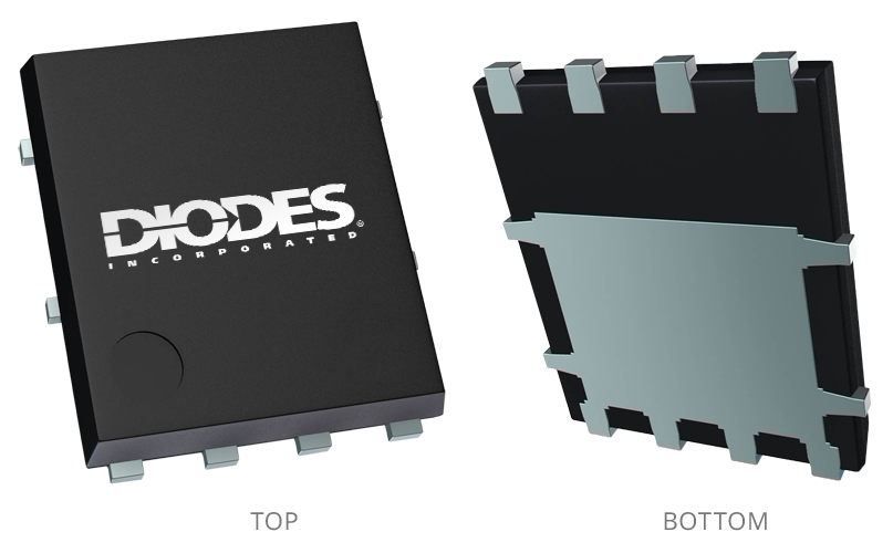
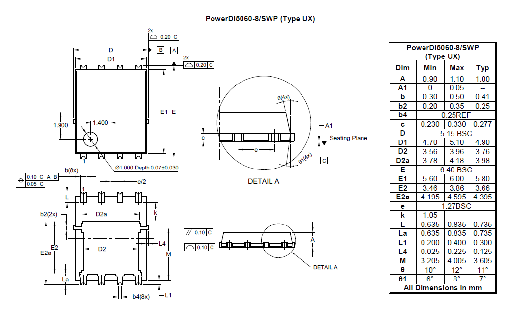
Image shown is for reference only. Actual package may vary. Refer to the product data sheet for package details. PowerDI5060-8
40V N-Channel Enhancement Mode MOSFET
Log in or register to manage email notifications about changes to datasheets or PCNs for this part.
This new generation N-Channel Enhancement Mode MOSFET is designed to minimize RDS(ON), yet maintain superior switching performance. This device is ideal for use in notebook battery power management and loadswitch.
Compliance (Only Automotive Supports PPAP) |
Standard |
|---|---|
AEC Qualified |
Yes |
Polarity |
N |
ESD Diodes (Y|N) |
No |
|VDS| (V) |
40 V |
|VGS| (±V) |
20 ±V |
|IDS| @TA = +25°C (A) |
15.7 A |
|IDS| @TC = +25°C (A) |
100 A |
PD @TA = +25°C (W) |
2.8 W |
PD @TC = +25°C (W) |
136 W |
RDS(ON)Max@ VGS(10V) (mΩ) |
7.6 mΩ |
|VGS(TH)| Min (V) |
2 V |
|VGS(TH)| Max (V) |
4 V |
QG Typ @ |VGS| = 10V (nC) |
41.9 nC |
CISS Typ (pF) |
2082 pF |
CISS Condition @|VDS| (V) |
25 V |
Something went wrong with your request. Please try again later. If this problem continues, please contact Diodes support for assistance.
A PCN may only apply to specific orderable part numbers in this datasheet. Please refer to the corresponding PCN to see the exact orderable part number(s) affected.
| PCN # | Issue Date | Implementation Date | Subject |
|---|---|---|---|
| PCN-2770 | 2025-10-30 | 2025-10-30 | Add Fab Site Code, Country of Diffusion (COD) and Assembly Site Origin (ASO) on Product and Shipping Labels for all Diodes Products |
