30V High Frequency Half-Bridge Gate Driver with Adaptive Deadtime in DFN3030-8
Log in or register to manage email notifications about changes to datasheets or PCNs for this part.
The DGD28225 is a high-frequency gate driver with an internal bootstrap diode capable of driving N-channel MOSFETs in a half-bridge configuration. the floating high-side driver is rated up to 30V in a bootstrap configuration.
System efficiency in the half-bridge is greatly improved with adaptive deadtime, 19ns rise and fall times, and 22ns propagation delays. UVLO for the high- and low-side protects the MOSFET during a loss of supply.
Fast and well-matched propagation delays and rise and fall times allow for a higher switching frequency, which enables a smaller, more compact power switching design using smaller associated components. To minimize component footprint, an internal boostrap diode is included.
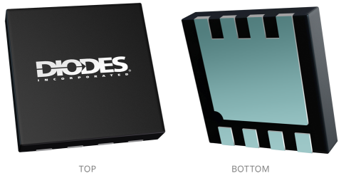
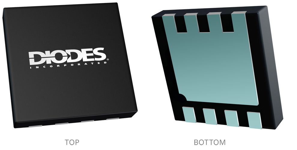
The DGD28225 is packaged in a space-saving U-DFN3030-8 package. The device’s operating temperature extends from -40°C to +125°C.
Offset Voltage Max (V) |
30 V |
|---|---|
Inputs |
PWM, EN/FO* |
Output Current IO+ (Typ) (mA) |
1500/1500 mA |
Output Current IO- (Typ) (mA) |
1500/2400 mA |
Internal Deadtime (Typ) |
22 ns |
tON (Typ) (ns) |
60 ns |
tOFF (Typ) (ns) |
22 ns |
tR (Typ) (ns) |
17 ns |
tF (Typ) (ns) |
17 ns |
A PCN may only apply to specific orderable part numbers in this datasheet. Please refer to the corresponding PCN to see the exact orderable part number(s) affected.
| PCN # | Issue Date | Implementation Date | Subject |
|---|---|---|---|
| PCN-2770 | 2025-10-30 | 2025-10-30 | Add Fab Site Code, Country of Diffusion (COD) and Assembly Site Origin (ASO) on Product and Shipping Labels for all Diodes Products |
