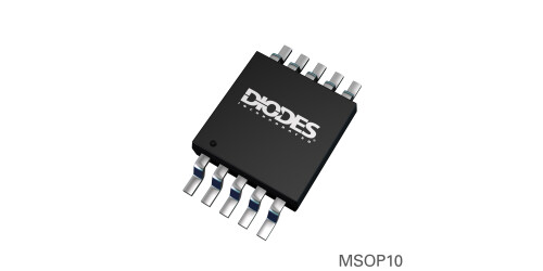
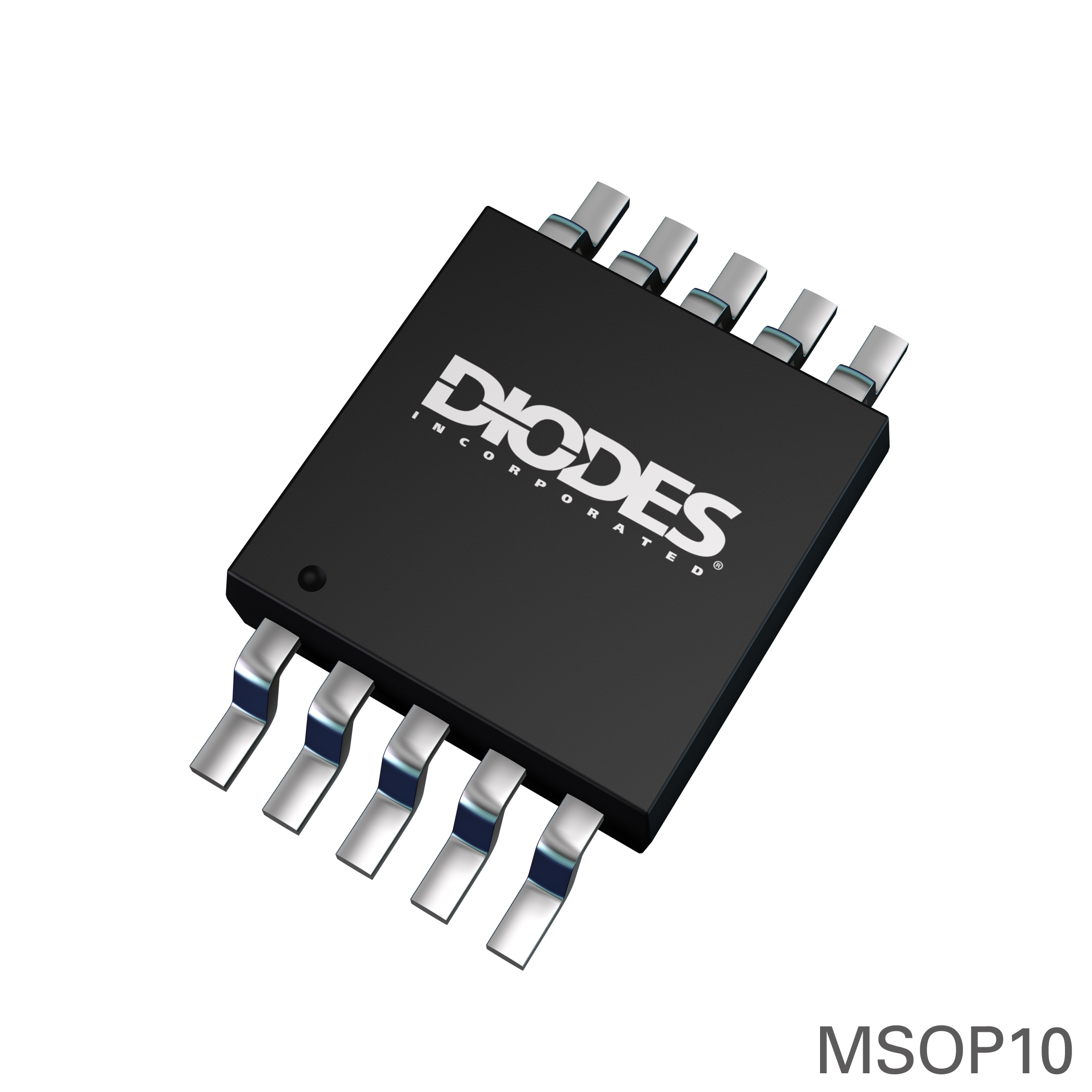
Image shown is for reference only. Actual package may vary. Refer to the product data sheet for package details. MSOP-10
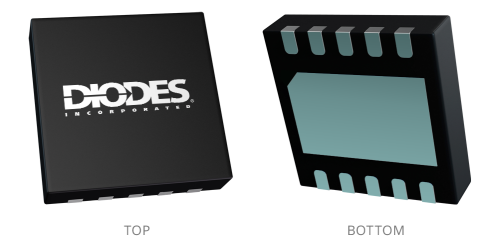
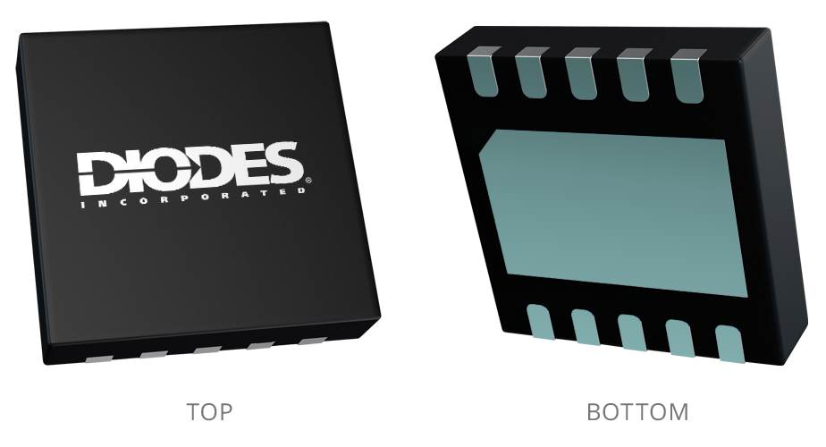
Image shown is for reference only. Actual package may vary. Refer to the product data sheet for package details. W-DFN3030-10 (Type TH)
NRND = Not Recommended for New Design
HIGH FREQUENCY HALF-BRIDGE GATE DRIVER WITH PROGRAMMABLE DEADTIME IN W-DFN3030-10
Log in or register to manage email notifications about changes to datasheets or PCNs for this part.
The DGD0506A is a high-frequency half-bridge gate driver capable of driving N-channel MOSFETs in a half-bridge configuration. The floating high-side driver is rated up to 50V.
The DGD0506A logic inputs are compatible with standard TTL and CMOS levels (down to 3.3V) to interface easily with MCUs. UVLO for high-side and low-side will protect a MOSFET with loss of supply. To protect MOSFETs, cross conduction prevention logic prevents the HO and LO outputs being on at the same time.
Fast and well-matched propagation delays allow a higher switching frequency, enabling a smaller, more compact power switching design using smaller associated components. The DGD0506A is offered in the W-DFN3030-10 (Type TH) package and operates over an extended -40°C to +125°C temperature range.
Inputs |
IN, EN |
|---|---|
Internal Deadtime (Typ) |
70 |
Offset Voltage Max (V) |
50 |
Output Current IO- (Typ) (mA) |
2000 |
Output Current IO+ (Typ) (mA) |
1500 |
tF (Typ) (ns) |
12 |
tOFF (Typ) (ns) |
22 |
tON (Typ) (ns) |
96 |
tR (Typ) (ns) |
17 |
Something went wrong with your request. Please try again later. If this problem continues, please contact Diodes support for assistance.
A PCN may only apply to specific orderable part numbers in this datasheet. Please refer to the corresponding PCN to see the exact orderable part number(s) affected.
| PCN # | Issue Date | Implementation Date | Subject |
|---|---|---|---|
| PCN-2770 | 2025-10-30 | 2025-10-30 | Add Fab Site Code, Country of Diffusion (COD) and Assembly Site Origin (ASO) on Product and Shipping Labels for all Diodes Products |
