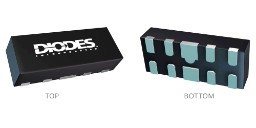
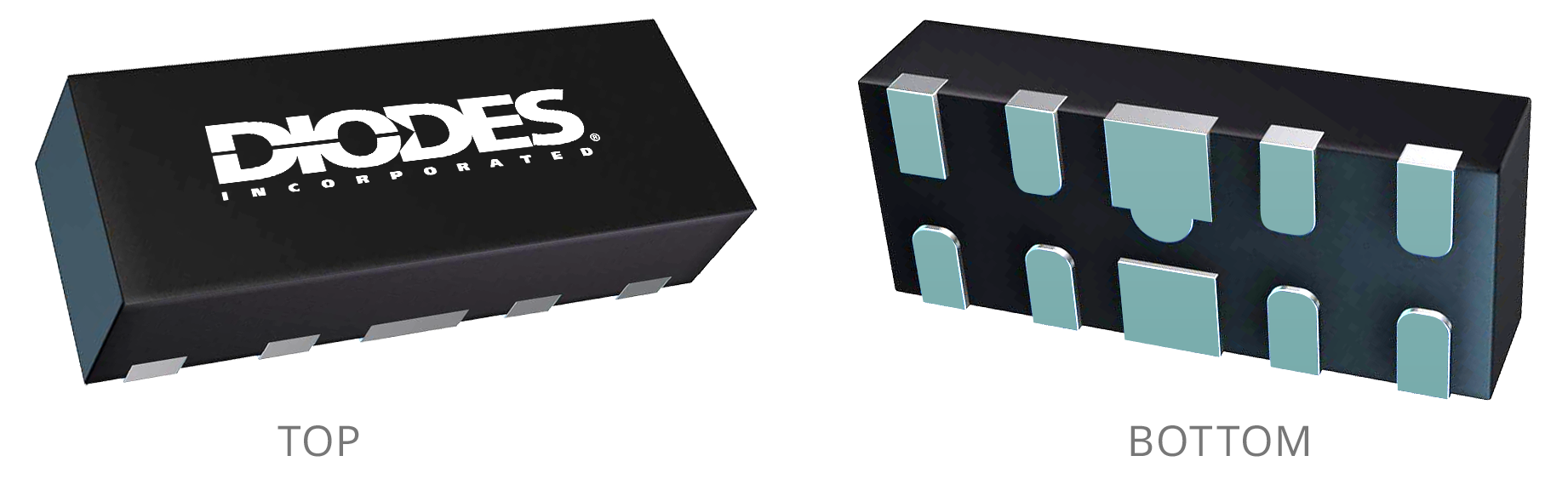
Image shown is for reference only. Actual package may vary. Refer to the product data sheet for package details. U-DFN2510-10
4 Channel Low Capacitance TVS Diode Array
Log in or register to manage email notifications about changes to datasheets or PCNs for this part.
The D3V3FA4U10LP is a high-performance device suitable for protecting four high-speed I/Os. It is engineered to protect sensitive electronic components from ESD events, which can occur during manufacturing, handling, or in the end-use environment. It is particularly suitable for high-speed data interfaces where maintaining signal integrity is crucial.
Compliance (Only Automotive Supports PPAP) |
Standard |
|---|---|
AEC Qualified |
No |
Configuration |
Uni-Directional |
Channel Input CapacitanceCT Typ (pF) |
0.4 pF |
Reverse Standoff Voltage VRWM(V) |
3.3 V |
Breakdown VoltageVBR Min(V) |
4 V |
Typ Reverse Leakage Current IR @ VRWM Max(µA) |
N/A µA |
Maximum Peak Pulse Current IPP @ 8x20μs Max |
4 |
Maximum Clamping Voltage @ Max Peak Pulse Current VC (V) |
11.5 V |
VESD IEC61000-4-2 Contact Discharge(kV) |
±20 kV |
Something went wrong with your request. Please try again later. If this problem continues, please contact Diodes support for assistance.
A PCN may only apply to specific orderable part numbers in this datasheet. Please refer to the corresponding PCN to see the exact orderable part number(s) affected.
| PCN # | Issue Date | Implementation Date | Subject |
|---|---|---|---|
| PCN-2770 | 2025-10-30 | 2025-10-30 | Add Fab Site Code, Country of Diffusion (COD) and Assembly Site Origin (ASO) on Product and Shipping Labels for all Diodes Products |
