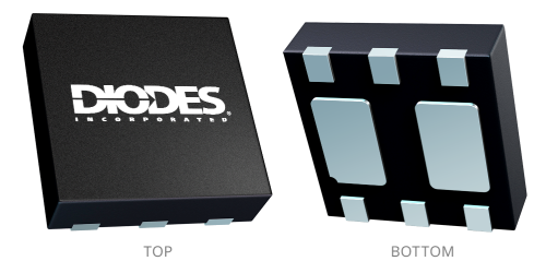
Image shown is for reference only. Actual package may vary. Refer to the product data sheet for package details. U-DFN2020-6 (Type B)
Switching Diode
Log in or register to manage email notifications about changes to datasheets or PCNs for this part.
Configuration |
Dual-Dual, Series (Alt.) |
|---|---|
CT(pF) Max @ VR = 0V, f = 1MHz |
2 |
ESD Diodes (Y|N) |
No |
Forward Voltage Drop VF @ IF (mA) |
50, 1 |
IR(nA) Max @ VR=5V |
10 |
IR(µA) Max @ VR=30V |
0.1 |
IR(uA) Max @ VR=80V |
2.5uA@75V |
Maximum Average Rectifier Current IO (mA) |
300 |
Maximum Peak Forward Surge Current IFSM (A) |
3 |
Maximum ReverseCurrent IR (µA) |
2.5 |
Maximum Reverse Current IR @ VR (V) |
75 |
Peak RepetitiveReverse VoltageVRRM (V) |
75 |
Polarity |
Anode, Cathode |
Power Rating(mW) |
500 |
AEC Qualified |
Yes |
Reverse RecoveryTime trr (ns) |
4 |
TotalCapacitance CT (pF) |
2 |
VF(V) Max @ IF=1.0mA |
0.7 |
VF(V) Max @ IF=100mA |
1.2 |
VF(V) Max @ IF=10mA |
0.82 |
Something went wrong with your request. Please try again later. If this problem continues, please contact Diodes support for assistance.
A PCN may only apply to specific orderable part numbers in this datasheet. Please refer to the corresponding PCN to see the exact orderable part number(s) affected.
| PCN # | Issue Date | Implementation Date | Subject |
|---|---|---|---|
| PCN-2770 | 2025-10-30 | 2025-10-30 | Add Fab Site Code, Country of Diffusion (COD) and Assembly Site Origin (ASO) on Product and Shipping Labels for all Diodes Products |
| PCN-2623 | 2023-05-15 | 2023-11-15 | Device End of Life (EOL) |
| PCN-2461 | 2020-05-08 | 2021-04-05 | Phenitec Wafer Manufacturing Site Change, Additional Wafer Sources, Wafer Diameter Change, Additional Assembly and Test Site |
