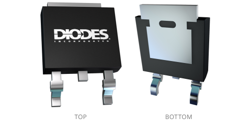
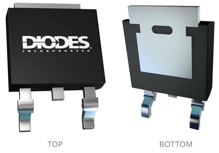
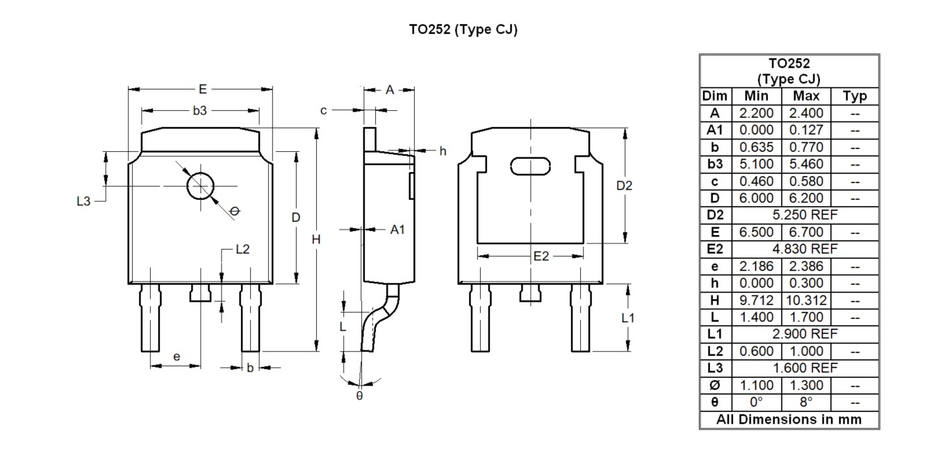
Image shown is for reference only. Actual package may vary. Refer to the product data sheet for package details. TO252 (DPAK)
High current, Wide Vin, 1 Amp LDO
Log in or register to manage email notifications about changes to datasheets or PCNs for this part.
The AZ1117I is available in industrial temperature range low dropout three-terminal regulator.
The AZ1117I is optimized for low voltage where transient response and minimum input voltage are critical. It provides current limit and thermal shutdown. Its circuit includes a trimmed bandgap reference to assure output voltage accuracy to be within ±1%. On-chip thermal shutdown provides protection against a combination of high current and ambient temperature that would create excessive junction temperature.
The AZ1117I is available in 1.2V, 1.5V, 1.8V, 2.5V, 3.3V, 5.0V fixed output voltage versions and ADJ output voltage version. The fixed versions integrate the adjust resistors. It is also available in an adjustable version which can set the output voltage with two external resistors.
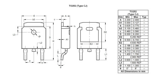
The AZ1117I is available in the industry-standard SOT223 and TO252-2 power package.
Iq (typ) (µA) |
4000 |
|---|---|
Iq (max) (µA) |
6000 |
Operating Ambient Temperature (°C) |
-40 to 125 |
AEC Qualified |
No |
Compliance (Only Automotive Supports PPAP) |
Standard |
Type |
LDO |
Output options |
Adjustable & Fixed |
Iout (A) |
1 |
Vin (Max) (V) |
15 |
Vin (Min) (V) |
3.2 |
Vout (min) |
1.25 |
Vout (max) |
15 |
Fixed Vout (V) |
1.2, 1.5, 1.8, 2.5, 3.3, 5.0 |
Adjustable VFB (V) |
1.25 |
Accuracy 25C |
1 |
Noise uV RMS 10-100 kHz |
150 |
VDROPOUT (Max) (V) at Max Current and Max Ouput Voltage |
1.4 |
PSRR (dB) 1kHz |
70 |
Enable Active |
No |
Channels |
1 |
Output Discharge |
No |
Power Good |
No |
Reverse Protection |
No |
VCTL Function |
No |
Something went wrong with your request. Please try again later. If this problem continues, please contact Diodes support for assistance.
A PCN may only apply to specific orderable part numbers in this datasheet. Please refer to the corresponding PCN to see the exact orderable part number(s) affected.
| PCN # | Issue Date | Implementation Date | Subject |
|---|---|---|---|
| PCN-2770 | 2025-10-30 | 2025-10-30 | Add Fab Site Code, Country of Diffusion (COD) and Assembly Site Origin (ASO) on Product and Shipping Labels for all Diodes Products |
| PCN-2761 | 2025-10-15 | 2025-10-15 | Add Ejector Pin Mark on TO-252 Packaged Products Manufactured at Diodes Internal Assembly and Test Site (SAT) |
| PCN-2568 | 2022-03-29 | 2022-03-29 | Qualified Additional Assembly & Test (A/T) Sites, Bill of Material, and updated Data Sheets for Package Outline Dimension Change |
| PCN-2514 | 2021-03-09 | 2021-06-09 | Additional Wafer Source JKFAB |
