2.0A Single Channel Load Switch With True Reverse Current Blocking
Log in or register to manage email notifications about changes to datasheets or PCNs for this part.
The AP22916 is a small, low leakage, single P-channel power MOSFET designed for low-power consumption and load-switching applications. This power MOSFET has a typical RDS(ON) of 60mΩ at 5V, allowing increased load current handling capacity with a low forward voltage drop. Multiple voltages correspond to different time options to support various system load conditions. The trigger of the load switch ON pin can be controlled to be enabled or disabled by an external low voltage digital signal for sequence control application. The smart, pull down feature is built into the ON pin. Once the enable voltage is higher than VIH, it will disconnect to avoid power loss. VIN and VOUT are isolated during OFF state with the TRCB (true reverse current blocking) feature.
The AP22916 load switch is designed to operate from 1.3V to 5.5V, making it ideal for 1.3V, 1.8V, 2.5V, 3.6V, and 5V systems. The typical quiescent supply current is only 0.5µA.
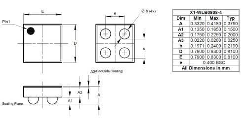
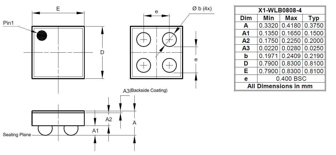
The AP22916 is available in the wafer-level chip-scale 4-pin, U-WLB0808-4 (Type B) 0.78mm x 0.78mm x 0.455mm, 0.4mm pitch package. The device is characterized for operation over a temperature range of -40°C to +85°C.
Type |
Load Switch |
|---|---|
AEC Qualified |
No |
Compliance (Only Automotive Supports PPAP) |
Standard |
Quiescent Current Typ (μA) |
0.3 |
Maximum Continuous Output Current (A) |
2 |
(MAX) Maximum Current Limit Fixed (A) |
Not Limited |
Channels |
1 |
Enable Logic |
Active High |
Minimum Operating Voltage (V) |
1.3 |
Maximum Operating Voltage (V) |
5.5 |
RDS(ON) (VIN = 5V) Typ (mΩ) |
54 |
Reverse Current Block |
Yes |
Minimum Power Supply Voltage (V) |
1.3 |
Maximum Power Supply Voltage (V) |
5.5 |
Output Discharge |
Yes |
(TYP) Output Rise Time mS |
0.05, 0.75 |
OCP Flag |
No |
Power Good |
No |
Overtemperature Protection |
Yes |
UL Certificate |
No |
A PCN may only apply to specific orderable part numbers in this datasheet. Please refer to the corresponding PCN to see the exact orderable part number(s) affected.
| PCN # | Issue Date | Implementation Date | Subject |
|---|---|---|---|
| PCN-2770 | 2025-10-30 | 2025-10-30 | Add Fab Site Code, Country of Diffusion (COD) and Assembly Site Origin (ASO) on Product and Shipping Labels for all Diodes Products |
