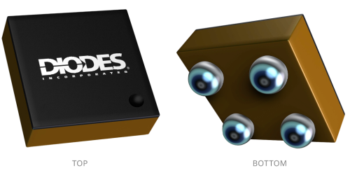
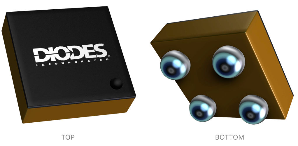
Image shown is for reference only. Actual package may vary. Refer to the product data sheet for package details. X1-WLB0909-4
Single Slew Rate Controlled Load Switch With True Reverse Current Blocking
Log in or register to manage email notifications about changes to datasheets or PCNs for this part.
The AP22913 slew rate controlled load switch is a single P-channel MOSFET power switch designed for high-side load-switchingapplications. The MOSFET has a typical RDS(ON) of 54mΩ at 5V (X1- WLB0909-4) and a typical RDS(ON) of 84mΩ at 5V (SOT26), allowing increased load current handling capacity with a low forward voltage drop. The turn-on slew rate of the device is controlled internally. VIN and VOUT are isolated during OFF state with TRCB (True Reverse Current Blocking) feature.
The AP22913 load switch is designed to operate from 1.4V to 5.5V, making it ideal for 1.8V, 2.5V, 3.3V and 5V systems. The typical quiescent supply current is only 1μA.
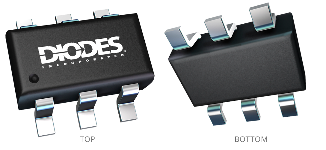
The AP22913 is available in the wafer level chip scale 4-pin, X1-WLB0909-4 0.5mm pitch and standard SOT26 packages.
Type |
Load Switch |
|---|---|
AEC Qualified |
No |
Compliance (Only Automotive Supports PPAP) |
Standard |
Quiescent Current Typ (μA) |
1 |
Maximum Continuous Output Current (A) |
2 |
(MAX) Maximum Current Limit Fixed (A) |
Not Limited |
Channels |
1 |
Enable Logic |
Active High |
Minimum Operating Voltage (V) |
1.4 |
Maximum Operating Voltage (V) |
5.5 |
RDS(ON) (VIN = 5V) Typ (mΩ) |
54, 84 |
Reverse Current Block |
Yes |
Minimum Power Supply Voltage (V) |
1.4 |
Maximum Power Supply Voltage (V) |
5.5 |
Output Discharge |
Yes |
(TYP) Output Rise Time mS |
0.66 |
OCP Flag |
No |
Power Good |
No |
Overtemperature Protection |
Yes |
UL Certificate |
No |
Something went wrong with your request. Please try again later. If this problem continues, please contact Diodes support for assistance.
A PCN may only apply to specific orderable part numbers in this datasheet. Please refer to the corresponding PCN to see the exact orderable part number(s) affected.
| PCN # | Issue Date | Implementation Date | Subject |
|---|---|---|---|
| PCN-2770 | 2025-10-30 | 2025-10-30 | Add Fab Site Code, Country of Diffusion (COD) and Assembly Site Origin (ASO) on Product and Shipping Labels for all Diodes Products |
| PCN-2700 | 2024-08-13 | 2024-11-11 | Additional Wafer Source - SPFAB |
| PCN-2531 | 2021-07-30 | 2022-01-29 | Additional Die Revision, Redistribution Layer (RDL), BUMP Sites (SJSEMI and LBS), as well as Assembly/Test (A/T) Site (CAT) |
