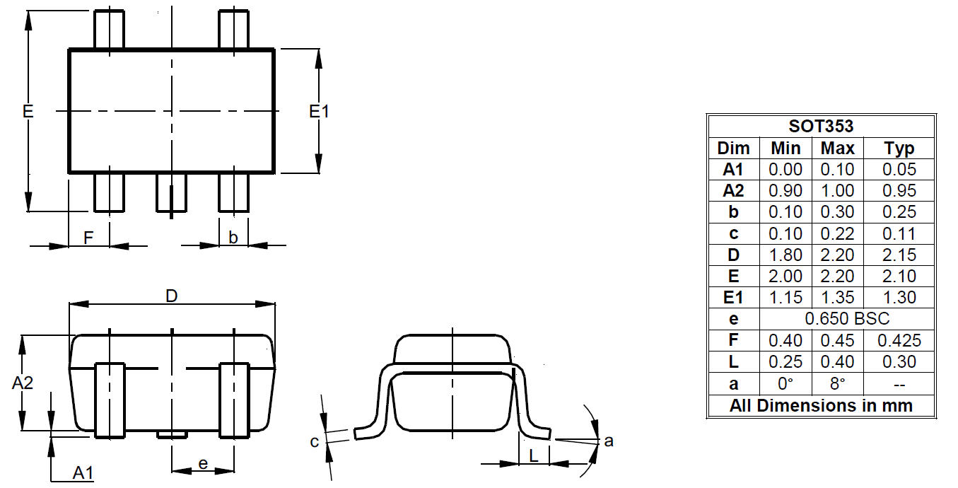
Image shown is for reference only. Actual package may vary. Refer to the product data sheet for package details. SC59
Image shown is for reference only. Actual package may vary. Refer to the product data sheet for package details. SOT23
Image shown is for reference only. Actual package may vary. Refer to the product data sheet for package details. SOT25
300MA, High Speed, Extremely Low Noise CMOS LDO Regulator
Log in or register to manage email notifications about changes to datasheets or PCNs for this part.
Iq (typ) (µA) |
60 |
|---|---|
Iq (max) (µA) |
90 |
Operating Ambient Temperature (°C) |
-40 to 85 |
AEC Qualified |
No |
Compliance (Only Automotive Supports PPAP) |
Standard |
Type |
LDO |
Output options |
Fixed |
Iout (A) |
0.3 |
Vin (Max) (V) |
6 |
Vin (Min) (V) |
2.3 |
Vout (min) |
1.8 |
Vout (max) |
4.2 |
Fixed Vout (V) |
1.8, 2.5, 2.8, 3.0, 3.3, 4.15, 4.2 |
Accuracy 25C |
2 |
Noise uV RMS 10-100 kHz |
50 |
VDROPOUT (Max) (V) at Max Current and Max Ouput Voltage |
0.3 |
PSRR (dB) 1kHz |
70 |
Enable Active |
Yes (High) |
Channels |
1 |
Output Discharge |
Yes |
Power Good |
No |
Reverse Protection |
No |
VCTL Function |
No |
Something went wrong with your request. Please try again later. If this problem continues, please contact Diodes support for assistance.
A PCN may only apply to specific orderable part numbers in this datasheet. Please refer to the corresponding PCN to see the exact orderable part number(s) affected.
| PCN # | Issue Date | Implementation Date | Subject |
|---|---|---|---|
| PCN-2770 | 2025-10-30 | 2025-10-30 | Add Fab Site Code, Country of Diffusion (COD) and Assembly Site Origin (ASO) on Product and Shipping Labels for all Diodes Products |
| PCN-2709 | 2025-01-07 | 2025-04-07 | Additional Wafer Source (GFAB), Die Revision, Data Sheet Change and Additional Bill of Materials (BOM) |
| PCN-2568 | 2022-03-29 | 2022-03-29 | Qualified Additional Assembly & Test (A/T) Sites, Bill of Material, and updated Data Sheets for Package Outline Dimension Change |
| PCN-2512 | 2021-04-16 | 2021-07-16 | Qualified Additional Assembly & Test (A/T) Site |
