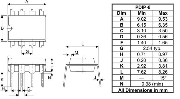
Image shown is for reference only. Actual package may vary. Refer to the product data sheet for package details. SO-8
NRND = Not Recommended for New Design
Log in or register to manage email notifications about changes to datasheets or PCNs for this part.
The AP1662 is an active power factor control IC which is designed mainly for use as a pre-converter in electronic ballast, AC-DC adapter and off-line SMPS applications. The IC includes an internal start-up timer for stand-alone applications, a one-quadrant multiplier to realize near unity power factor and a zero current detector to ensure DCM boundary conduction operation. The totem pole output stage is capable of driving power MOSFET with 600mA source current and 800mA sink current. Designed with advanced BiCMOS process, the AP1662 features low start-up current, low operation current and low power dissipation. The AP1662 also has rich protection features including over-voltage protection, input under-voltage lockout with hysteresis and multiplier output clamp to limit maximum peak current. The AP1662 meets IEC61000-3-2 standard even at one-quadrant load and THD lower than 10% at high-end line voltage and full load.
Accuracy (%) |
2 |
|---|---|
Dimming |
N/A |
Efficiency (%) |
90 |
Frequency (kHz) |
N/A |
LED Current (mA) |
External MOSFET |
Maximum DC VDD (VDC) |
N/A |
Minimum Input AC Voltage (VAC) |
85 |
SupplyCurrent (mA) |
3.5 |
Temperature Range (°C) |
-40 to 105 |
Something went wrong with your request. Please try again later. If this problem continues, please contact Diodes support for assistance.
A PCN may only apply to specific orderable part numbers in this datasheet. Please refer to the corresponding PCN to see the exact orderable part number(s) affected.
| PCN # | Issue Date | Implementation Date | Subject |
|---|---|---|---|
| PCN-2770 | 2025-10-30 | 2025-10-30 | Add Fab Site Code, Country of Diffusion (COD) and Assembly Site Origin (ASO) on Product and Shipping Labels for all Diodes Products |
