NRND = Not Recommended for New Design
High Efficiency 1x/2x Charge Pump LED Driver
For Small Screen
Log in or register to manage email notifications about changes to datasheets or PCNs for this part.
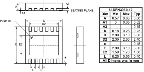
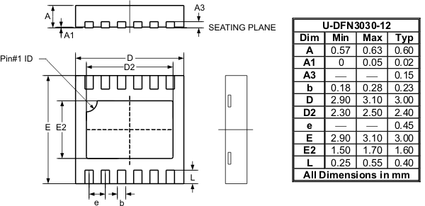
The AL3157 is a low noise, constant frequency charge pump DC/DC converter that uses a Dual mode load switch (1x), and doubling (2x) conversion for driving white LEDs. Low external part count (one 1µF flying capacitor and two 2.2µF capacitors at VIN and VOUT) make this part ideally suited for small, battery-powered applications The AL3157 drives 3 channels at up to 30mA for small screen backlighting and an additional channel up to 210mA for LED Flash or LED Flashlight – All from a 2.7V to 5.5V input. The AL3157 uses two control inputs (EN1/2) to enable/disable it and PWM dim the LED current. EN2 controls/PWM dims the backlight LEDs at 30mA per channel and EN1 controls/PWM dims the Flash/Flashlight LEDs at 210mA. Each output of the AL3157 is equipped with built-in protection for VOUT short circuit and auto-disable for LED failure conditions. Built-in soft-start circuitry prevents excessive in-rush current during start-up and mode switching. A low-current shutdown feature disconnects the load from VIN to reduce quiescent current less than 1µA. The AL3157 is available in a lead-free, space-saving, thermally enhanced 12-pin 3 x 3mm DFN package.
AEC Qualified |
No |
|---|---|
AEC-Q100 Grade |
No |
Compliance (Only Automotive Supports PPAP) |
Standard |
Dimming |
PWM |
Dimming (Analog) |
No |
Dimming (PWM) |
No |
Efficiency (%) |
93 |
Efficiency (%) |
93 |
Function |
Charge Pump LED Driver |
LED Current (A) |
0.21 |
MaximumInput Voltage (V) |
5.5 |
Maximum LED Current (A) |
0.21 |
Maximum Output Current per Channel |
210 |
Maximum Output Voltage (V) |
5.5 |
Maximum Output Voltage (V) |
5.5 |
MinimumInput Voltage (V) |
2.7 |
Number of Regulated Output Channels |
4 |
OperatingTemperatureRange (°C) |
-40 to 85 |
Operating Temperature Range (°C) |
-40 to 85 |
OVP |
Yes |
AEC Qualified |
No |
Quiescent Current (µA) |
2 |
Quiescent Current Typ (μA) |
2 |
Quiescent Current Typ (mA) |
2 |
Soft Start |
Yes |
Standby Quiescent Current (µA) |
1 |
SW RDS(ON) |
0.5 |
Switching Frequency (MHz) |
1.2 |
Switching Frequency Maximum (kHz) |
1.2 |
Topologies (Boost) |
No |
Topologies (Buck-Boost) |
No |
Topologies (Buck) |
No |
Topologies (SEPIC) |
Yes |
Topology |
Charge Pump |
Typical Overcurrent Protection Current |
N/A |
VFB |
N/A |
Something went wrong with your request. Please try again later. If this problem continues, please contact Diodes support for assistance.
A PCN may only apply to specific orderable part numbers in this datasheet. Please refer to the corresponding PCN to see the exact orderable part number(s) affected.
| PCN # | Issue Date | Implementation Date | Subject |
|---|---|---|---|
| PCN-2770 | 2025-10-30 | 2025-10-30 | Add Fab Site Code, Country of Diffusion (COD) and Assembly Site Origin (ASO) on Product and Shipping Labels for all Diodes Products |
