4-Bit Dual Power Supply Translating Buffer with 3-State Outputs
Log in or register to manage email notifications about changes to datasheets or PCNs for this part.
The 74AVCH4T245 device is 4-bit, dual supply transceiver that enables bidirectional level translation, designed for asynchronous communication between two data buses. It features four 2-bit input-output ports (nAn and nBn), a direction control input (nDIR), an output enable input (nOE) and dual supply pins (VCC(A) and VCC(B)). Both VCC(A) and VCC(B) can be supplied at any voltage between 0.8 V and 3.6 V making the device suitable for translating between any of the low voltage nodes (0.8V, 1.2V, 1.5V, 1.8V, 2.5V and 3.3V). Pins nAn, nOE and nDIR are referenced to VCC(A) and pins nBn are referenced to VCC(B). A HIGH on nDIR allows transmission from nAn to nBn and a LOW on nDIR allows transmission from nBn to nAn. The output enable input (nOE) can be used to disable the outputs so the buses are effectively isolated. The device is fully specified for partial power-down applications using IOFF. The IOFF circuitry disables the output, preventing any damaging back flow current through the device when it is powered down. In suspend mode when either VCC(A) or VCC(B) are at GND level, both nAn and nBn are in the high-impedance OFF-state. The 74AVCH4T245 has active bus hold circuitry which is provided to hold unused or floating data inputs at a valid logic level. This feature eliminates the need for external pull-up or pull-down resistors.
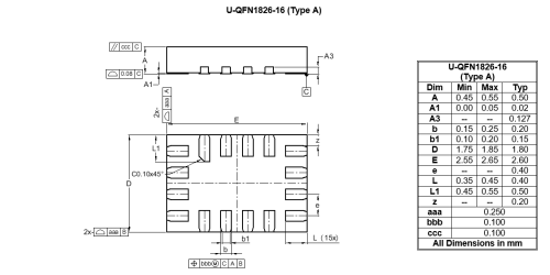
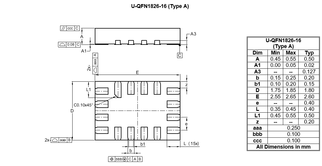
The 74AVCH4T245 is available in the packages, and is specified for operation from -40°C to +125°C among all supply voltages. The wide temperature ranges and high ESD tolerance facilitate their use in harsh applications.
Compliance (Only Automotive Supports PPAP) |
Standard |
|---|---|
Translation From (V) |
0.8 to 3.6 |
Translation To (V) |
0.8 to 3.6 |
Max Signal Rate |
380Mbps |
Bits Needed |
4 |
Auto Direction Sensing? |
No |
Shift |
DIR-Control |
Prop Delay (ns) |
2.8 |
Ambient or Junction Temperature (°C) |
-40 to 125 |
Additional Technical Documents are available upon request:
Application information, Evaluation board, and Other technical documents
Something went wrong with your request. Please try again later. If this problem continues, please contact Diodes support for assistance.
A PCN may only apply to specific orderable part numbers in this datasheet. Please refer to the corresponding PCN to see the exact orderable part number(s) affected.
| PCN # | Issue Date | Implementation Date | Subject |
|---|---|---|---|
| PCN-2770 | 2025-10-30 | 2025-10-30 | Add Fab Site Code, Country of Diffusion (COD) and Assembly Site Origin (ASO) on Product and Shipping Labels for all Diodes Products |
