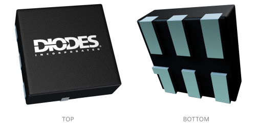
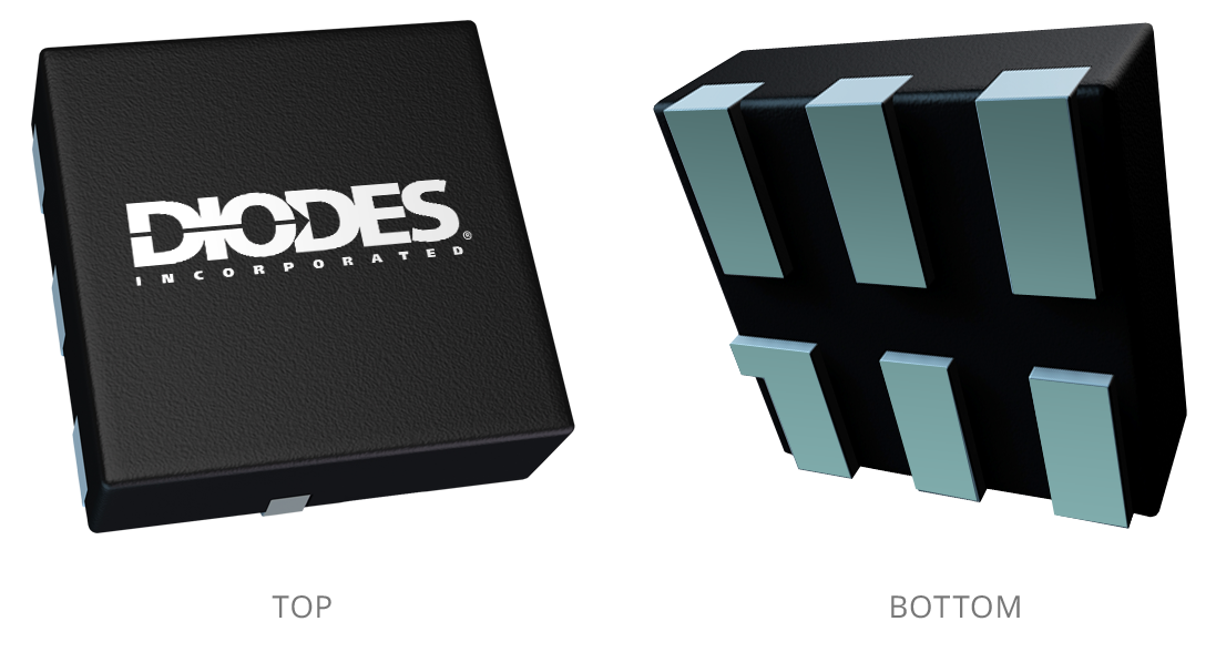
Image shown is for reference only. Actual package may vary. Refer to the product data sheet for package details. X2-DFN1010-6
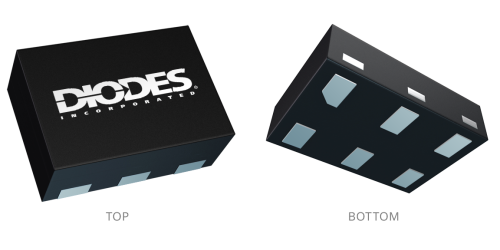
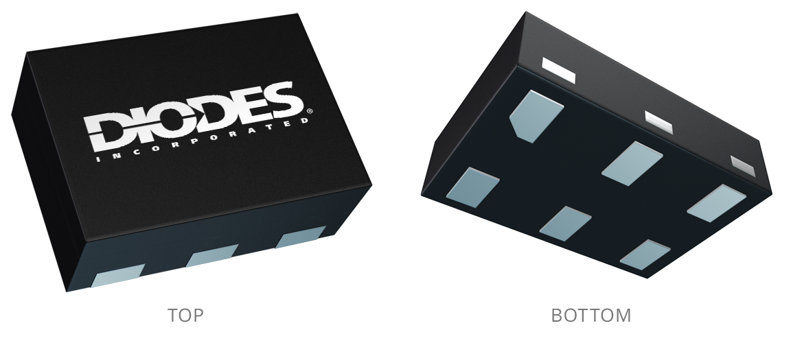
Image shown is for reference only. Actual package may vary. Refer to the product data sheet for package details. X2-DFN1410-6
Single Bit Dual Power Supply Translating Buffer with 3 State Outputs
Log in or register to manage email notifications about changes to datasheets or PCNs for this part.
The 74AUP1T34 is a single-bit, dual-supply, noninverting buffer translator suitable for transmitting a single logic bit across different voltage domains. It is a unidirectional translator from A to Y. The input pin A has input switching thresholds related to VCCA, operating from 0.9V to 3.6V. The output pin Y has a HIGH level output voltage that tracks VCCB, also operating from 0.9V to 3.6V. This arrangement allows for universal low-voltage translation between any voltages from 0.9V to 3.6V.
The three-state feature occurs when the VCCA power-supply voltages are zero. This is also an IOFF feature and allows the output to remain in a high-impedance state, preventing damaging backflow currents and providing power-down electrical isolation of up to 3.6V. If the VCCB is at ground, the input circuits at pin A are disabled and no input current flows regardless of any applied voltage between 0V and 3.6V.
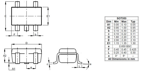
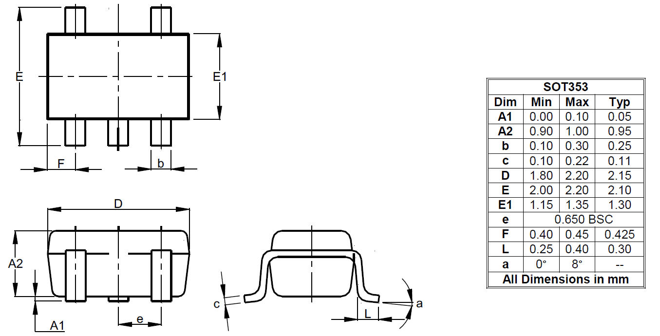
The 74AUP1T34 is available in the SOT353, X2-DFN1410-6, and X2- DFN1010-6 packages, and is specified for operation from -40°C to +125°C among all supply voltages. The wide temperature ranges and high ESD tolerance facilitate their use in harsh applications.
Function |
Transceiver |
|---|---|
Type |
Buffers/Inverters/Transceivers |
Compliance (Only Automotive Supports PPAP) |
Standard |
Channels |
1 |
Family |
AUP |
VCC Min (V) |
0.9 |
VCC Max (V) |
3.6 |
Input Type |
Standard CMOS |
Output Type |
3-State |
Output Current (mA) |
50 |
Something went wrong with your request. Please try again later. If this problem continues, please contact Diodes support for assistance.
A PCN may only apply to specific orderable part numbers in this datasheet. Please refer to the corresponding PCN to see the exact orderable part number(s) affected.
| PCN # | Issue Date | Implementation Date | Subject |
|---|---|---|---|
| PCN-2770 | 2025-10-30 | 2025-10-30 | Add Fab Site Code, Country of Diffusion (COD) and Assembly Site Origin (ASO) on Product and Shipping Labels for all Diodes Products |
