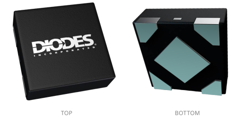
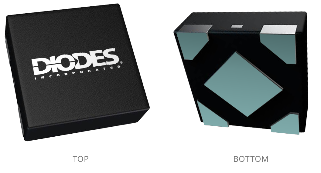
Image shown is for reference only. Actual package may vary. Refer to the product data sheet for package details. X2-DFN1010-4 (Type B)
250MA High PSRR Low Noise LDO with ENABLE
Log in or register to manage email notifications about changes to datasheets or PCNs for this part.
The AP7353 is a low dropout regulator with high output voltage accuracy, low RDSON, high PSRR, low output noise and low quiescent current. This regulator is based on a CMOS process.
The AP7353 includes a voltage reference, error amplifier, current limit circuit and an enable input to turn it on and off. With the integrated resistor network, fixed output voltage versions can be delivered.
With its high PSRR, good line regulation and fast load transient response, the AP7353 is well suited for handheld/wearable
communication equipments which require stable voltage sources.
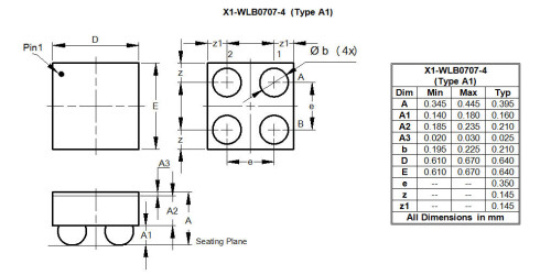
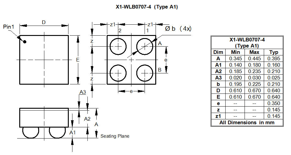
The AP7353 is packaged in X1-WLB0707-4 (Type A1) which allows for smallest footprint and dense PCB layout.
Iq (typ) (µA) |
18 |
|---|---|
Iq (max) (µA) |
27 |
Operating Ambient Temperature (°C) |
-40 to 85 |
AEC Qualified |
No |
Compliance (Only Automotive Supports PPAP) |
Standard |
Type |
LDO |
Output options |
Fixed |
Iout (A) |
0.25 |
Vin (Max) (V) |
5.5 |
Vin (Min) (V) |
2 |
Vout (min) |
1.8 |
Vout (max) |
4.5 |
Fixed Vout (V) |
1.8, 2.5, 2.8, 2.85, 2.9, 3.0, 3.1, 3.2, 3.3, 3.6, 4.5 |
Accuracy 25C |
1 |
Noise uV RMS 10-100 kHz |
10 |
VDROPOUT (Max) (V) at Max Current and Max Ouput Voltage |
0.117 |
PSRR (dB) 1kHz |
90 |
Enable Active |
Yes (High) |
Channels |
1 |
Output Discharge |
Yes, No |
Power Good |
No |
Reverse Protection |
No |
VCTL Function |
No |
Something went wrong with your request. Please try again later. If this problem continues, please contact Diodes support for assistance.
A PCN may only apply to specific orderable part numbers in this datasheet. Please refer to the corresponding PCN to see the exact orderable part number(s) affected.
| PCN # | Issue Date | Implementation Date | Subject |
|---|---|---|---|
| PCN-2770 | 2025-10-30 | 2025-10-30 | Add Fab Site Code, Country of Diffusion (COD) and Assembly Site Origin (ASO) on Product and Shipping Labels for all Diodes Products |
| PCN-2568 | 2022-03-29 | 2022-03-29 | Qualified Additional Assembly & Test (A/T) Sites, Bill of Material, and updated Data Sheets for Package Outline Dimension Change |
