
Advanced PCIe Features for Power-Conscious and Mission-Critical Applications

By: Jen Lee, Marketing Director
Multi-Talented Connectivity
PCI Express®(PCIe®) has become the interconnect of choice for the server, storage, and network market — and its appeal is also extending to backbone and I/O applications in industrial automation, IoT, consumer devices, and automotive electronics. To meet the user expectations and eco-design demands that apply in these sectors, the PCI Special Interest Group (PCI-SIG) introduced various power-saving innovations as well as features to improve reliability, availability, and serviceability (RAS) in successive generations of the specification.
Today’s PCIe 3.0 switches, which support data speeds up to 8GT/s per lane, combine generous bandwidth and up-to-the-minute power-management and RAS features to meet the needs of mobile and embedded applications.
Lowering Power Consumption
With the growth in portable, mobile, and IoT applications seeking to leverage PCIe’s attributes, the power consumption of the interconnect when the device is in both active and in standby has become increasingly important. The scalability of PCIe is one aspect that lets designers tailor the interface bandwidth and power consumption in active modes to suit their application. Diodes Incorporated offers a family of PCIe 3.0 switches that include the PI7C9X3G606GP, PI7C9X3G808GP, and PI7C9X3G816GP — which provide six, eight, and sixteen lanes of PCIe 3.0 connectivity respectively.
From the PCIe 3.0 generation, various link states are defined by the Link Training and Status State Machine (LTSSM). It allows power consumption when active, and when inactive, this is significantly reduced without impacting system performance.
L0 is the power state of a link that is operating normally. If no data is being transferred, the link can enter the L1 state, which turns off portions of the PCIe transceiver logic. Adding to the granularity, there are also L0s that allow two devices on a link to power down their transmitters independently when data is transferred in only one direction.
Recognizing that the physical layer also contains analog circuitry that continues to consume several milliwatts per lane even when idle, additional L1 sub-states have been defined that turn off the analog elements to maximize power savings. In the L1.1 sub-state, the transceiver PLL is turned off, while L1.2 turns off common-mode voltage keepers to reduce power further. The trade-off for taking advantage of the L1.1 and L1.2 lower-power states is that the resume latency is extended. Table 1 describes the features and performance of L1 and the L1.1/L1.2 sub-states.
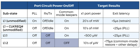
Table 1. L1 and L1 sub-states power-saving and performance comparison. (Source: https://www.synopsys.com/designware-ip/technical-bulletin/reduce-power-consumption.html)
To help manage this and ensure the link enters the most suitable low-power state to resume operation when needed, Latency Tolerance Reporting (LTR) enables the host to determine the maximum time to wait before servicing an interrupt from any given device. There is also the Optimized Buffer Flush/Fill (OBFF), which enables the host to message devices with system-state information. This permits the host processor and memory subsystem to power down and remain in the low-power state for longer to maximize energy savings.
There are additional low-power states, including L2, in which the transceiver is turned fully off, and L3, where the transceiver is turned off and power is removed. These help to minimize the power consumed by the PCIe interconnect circuitry when a device is idle. This is important for IoT applications, as well as equipment such as laptops and tablets to avoid draining the battery when the device is not being used.
Diodes’ PCIe switches, the PI7C9X3G606GP, PI7C9X3G808GP, and PI7C9X3G816GP, support these low-power link states and sub-states and can also turn off any empty hot-pluggable ports until they are needed. With power management schemes for startup and continuous operation, they draw very low power in all modes. Under full load and 80°C junction temperature, the PI7C9X3G808GP draws only 2.9W. The devices are specified over the industrial temperature range: -40°C to 85°C.
These switches also have a unique built-in PCIe 3.0 clock buffer that helps designers optimize application functionality and performance. The buffer supports various PCIe 3.0 reference clock architectures, including common, separate-reference no-spread (SRNS), and separate-reference independent-spread (SRIS).
 Addressing RAS in PCIe
High reliability, availability, and serviceability are key requirements in applications that are mission-critical and possibly safety-critical, such as in certain IoT and robotics applications. Mechanisms are needed to ensure the interface can operate correctly despite changing internal or external conditions, and can recover and resume normal operation after data errors.
Ensuring end-to-end data integrity is an underlying requirement, covered by various basic and optional features of the PCIe specifications. These include a 32-bit link-by-link cyclic redundancy code (LCRC) to detect errors, with an acknowledge mechanism (ACK/NACK) that allows replays to be requested. An acknowledge timeout confirms that the link partner is operating correctly and allows the link to be retrained if not received. There is also a transaction-layer 32-bit CRC (ECRC) for end-to-end data integrity detection. In addition, failsafe mechanisms for potential timeouts ensure that link partners return to a known state and that the LTSSM reinitializes.
Advanced Error Reporting (AER) is an optional PCIe capability that extends error signaling and logging. Error registers show the status of individual errors on a PCIe device function, indicating the severity and source of the error and allowing assessment of correctable and uncorrectable errors. This permits the system to detect failures and enter a safe state.
In addition to supporting these data-integrity features, Diodes’ PI7C9X3G606GP, PI7C9X3G808GP, and PI7C9X3G816GP also support provisions in the PCIe specification to handle surprise hot removal of a connected device. When a device is removed, normal responses based on request timeouts are slow, may result in data errors, and cause a task to crash or hang. Surprise hot removal avoids these errors by ensuring fast response when removal is detected.
These switches also support PCIe’s downstream port containment (DPC) option forhandling uncorrectable errors. DPC-capable ports automatically disable a link when an uncorrectable error is detected. This prevents the spread of corrupted data and enables the device to be removed. After removal, status flags are cleared, and the link can retrain for a newly connected device. The switches also provide hot-plug support for upstream/downstream ports and serial/parallel hot-plug types.
Other features include support for cross-domain end-point (CDEP) mode, in which one port is configured as a CDEP to connect to another host rather than an endpoint. This may be used to provide failover redundancy, or to allow communication between two processors or between a processor and an intelligent adaptor configured in processor mode. Each device also has four physical direct memory access (DMA) channels, which increase the efficiency of data interactions between the host and endpoints. These physical channels can be shared to let eight pairs of locations transfer data simultaneously.
 Conclusion
The popularity of PCIe is spreading beyond data centers, servers, and PCs and into broader domains, which include industrial, IoT, and consumer markets. The latest specifications introduce enhanced features to minimize power consumption and boost RAS. PCIe switches that support these features help system designers leverage the speed and versatility of this interconnect in power-conscious and mission-critical applications.
This article originally appeared in eBOM in June, 2022.