Signal Integrity in a GHz World
By: Chris A. Ciufo, Editor-in-Chief, Embedded, Extension Media Publishing
Two sets of dynamics are on a collision course making an often overlooked technical detail—signal integrity on PCBs, cables, connectors, and IC chip sets—more important than ever. When clocks and switching speeds were in the hundreds of megahertz, digital signals implemented in standards like 10/100 Ethernet, USB 2.0, SCSI, PCI and others behaved as expected and systems functioned per spec.
Spin the dial up into the gigahertz range and signal integrity becomes a major issue for designers. Smaller mobile devices crammed full of the latest high speed processors and I/O interfaces, coupled with die-shrunk multi-gigahertz processors and peripherals, mean signals get attenuated due to losses, cross coupling, and the low-cost PCBs and connectors common at consumer price points.
The silver bullet to solving these technical challenges is the repeater or redriver device. This inexpensive marvel added to the signal channel drives longer traces across FR4, through flex/ribbon cables, across backplanes, and meets eye diagram margins in all high-speed open standard interfaces. Let’s first examine the dynamics creating signal integrity challenges then see how the redriver solves signal integrity problems.
The Technology Dynamic
One dynamic is the relentless march of technology markets. CPU and endpoint peripheral controller speeds get faster all the time and GHz clocks are the norm. At the same time, IC’s pack more transistors onto the same size die through process shrinks and smaller feature sizes. Smaller transistors operate at lower voltages, offering lower output drive capability and an inability to move signals down long or high impedance lines.
Intel’s roadmap exemplifies rapid die shrinks, moving from 45nm in 2007 to 22nm today (Figure 1). For example, the Core Duo that replaced popular Pentium processors shipped in 65nm lithography while today’s 4th Generation Core i7 (Haswell) devices ship in 22nm (Figure 2).
As shown in Figure 3, Intel’s very small 22nm FinFET three-dimensional process packs in more transistors per cubic die millimeter, but has reduced operating gate voltages by an additional 0.2V. This is a whopping 20% reduction, and there’s a corresponding reduction in output drive capability for I/O like Ethernet, PCI Express, USB 3.0, SATA 3.0, SAS 2.0/3.0, and DDR memory. In three years, Intel expects 7nm transistors by 2017 and they’ll likely operate at a fraction of today’s Vdd voltages. Output drive capability will suffer even more.
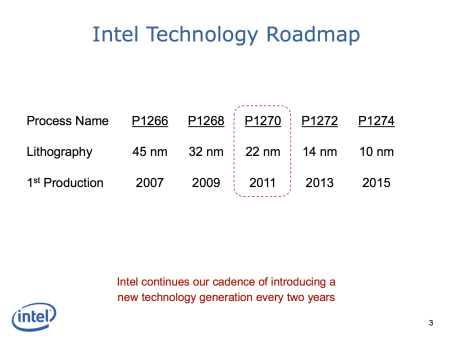
Figure 1: Intel’s lithography process roadmap. Note that these dates represent technology milestones; devices actually shipping in these technologies followed up to 24 months later. (Courtesy: Intel.)
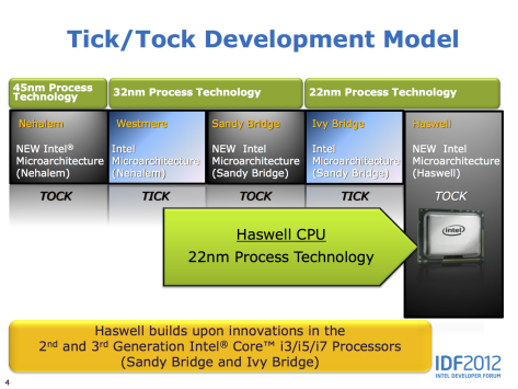
Figure 2: Intel’s CPU roadmap. (Courtesy: Intel.)
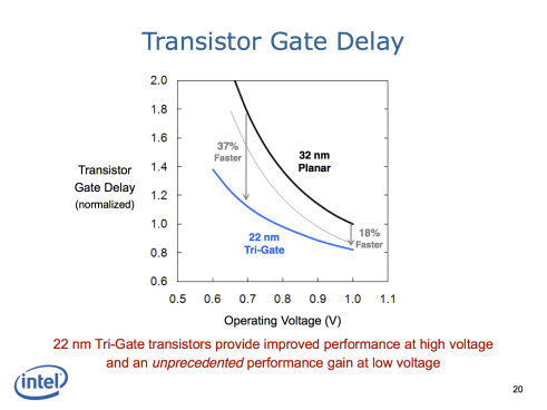
Figure 3: The move from planar transistors at 32nm to much faster three-dimensional 22nm Tri-Gate (FinFET) MOSFETs reduced gate voltages by 20 percent to around 0.8V. (Courtesy: Intel.)
Occurring in parallel with the trend to small, output signals are clocking faster, too. In 2002 PCI Express 1.0 ran 2.5 GT/s (gigatransfers/s). PCIe 2.0 doubled that to 5 GT/s while PCIe 3.0 is 8 GT/s (Figure 4). According to the PCISIG, PCIe 4.0 is targeting 16 GT/s by next year in 2015. Figure 5 shows similar increases in other SERDES standards.
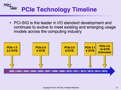
Figure 4: PCI Express just keeps getting faster. (Courtesy: PCISIG.)
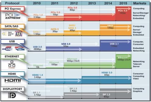
Figure 5: Serial standards roadmaps. Faster speeds mean signal integrity challenges.
These speeds exacerbate signal integrity problems exponentially. PCI Express 3.0 will tolerate a max channel loss of 20 dB: roughly 18 inches in FR4. With circuitous on-board routing, vias, connectors, risers and backplanes, non-handheld platforms will be quickly out of spec. Put another way, the move from 2.5 Gbits/s to 8 Gbits/s triples attenuation from 0.3 dB/inch to 0.9 dB/inch (FR4). In short: PCIe 3.0 simply won’t work properly in this system example without signal integrity mitigation techniques. In handhelds, trace lengths might not exceed 18 inches, but other PCB and chipset factors become equally significant.
The Platform Dynamic
Another dynamic affecting signal integrity is the platform race from desktop computing to mobile where tablets, smartphones, 2:1’s (tablet plus separate keyboard) and wearables are obsessively shrinking platforms and their internal boards. Devices sit closer than ever to each other, multilayer boards with stubs and buried vias struggle to route high fanout SoCs and peripherals, and space economization often mounts non-trivial ICs on flex circuits or even in stacked-chip multichip modules (MCMs)—or wherever there’s available space. In mobile platforms, despite their small external size, long and interrupted trace lengths are possible. Routing takes a back seat to real estate; signal integrity is often third priority if it’s considered at all.
For example, both micro HDMI and USB 3.0 are common in high-end smartphones. Case ergonomics may necessitate external connectors for these standards at non-ideal distances from the respective transmitter peripheral controllers. The connectors might not even be on the motherboard; rather, it’s possible they attach via internal cable or flex circuit. USB 3.0 signals that might be marginal at the case connector will be unacceptable at the other end of a user-connected cable. FR4 dielectric losses are 0.4 dB/inch at 5 GHz and total PCB attenuation in a large “phablet”-sized smartphone could conceivably exceed several dB.
Mobile devices have another unique challenge caused by extremely dense miniature mother and daughter boards routing gigahertz signals on narrowly spaced traces. Cross-coupling will occur due to proximity and skin effects. In such a small space, multiple distributed clock lines will pick up noise since source clocks can’t always be close to transceiver ICs, causing random jitter on data lines. This kind of jitter will run concurrently with data signals, adversely affecting the signal integrity that was already adversely affected by FR4 losses and impedance mismatches!
In other words: small packages like mobile compound signal integrity problems.
It All Adds Up Adversely
Both of these dynamics—platform changes and technology evolution—have adverse affects on signal integrity. Board layouts and mechanical considerations increase jitter, clocks degrade, attenuation builds, impedance problems cascade, and second and third order transmission line phenomena like the skin effect and narrow spacing coupling become non-trivial.
As signals degrade, bit-error rates increase and the margin built into the specs in Figure 5 is wiped out, resulting in poor video quality, data loss, retry errors, and degraded speeds. Even new specs targeting mobile like the PCISIG’s M-PCIe Gear 3 running M-PHY (5 – 5.8 Gbits/s) will encounter signal integrity challenges. As well, Moore’s Law speeds up ICs but they’re less capable of driving long, lossy traces and channels.
Underlying all of these concerns and at the back of designers’ minds is cost. Exotic PCB materials and high-quality RF-like connectors can sometimes mitigate a few of these challenges, but at what cost in platforms designed for low-cost consumer applications? Regardless, choosing an IC leaves little choice: its electrical characteristics are predefined.
Is there a way out of this signal integrity challenge?