Diodes Incorporated
W FLGA2520 17

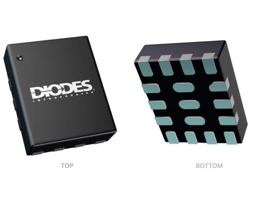
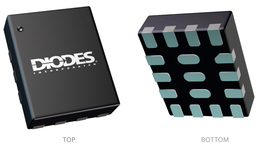
Image shown is for reference only. Actual package may vary. Refer to the product data sheet for package details.

W-FLGA2520-17.png
Back to Inactve Datasheet Archive

PAM2322AGEAR (Obsolete)

Dual High-Efficiency PWM Step-Down DC-DC Converter

Contact Sales

Log in or register to manage email notifications about changes to datasheets or PCNs for this part.

Description

The PAM2322AGEAR is a dual step-down current-mode, DC-DC converter. At heavy load, the constant-frequency PWM control performs with excellent stability and transient response. To ensure the longest battery life in portable applications, the PAM2322AGEAR provides a power-saving Pulse-Skipping Modulation (PSM) mode to reduce quiescent current under light load operation
 
The PAM2322AGEAR supports a range of input voltages from 2.7V to 5.5V, allowing the use of a single Li+/Li-polymer cell, multiple Alkaline/NiMH cell, USB, and other standard power sources. Output 1 is a 1.8V fixed output. Output 2 is adjustable from 0.9V to VIN. Both outputs employ an internal power switch and synchronous rectifier to minimize external part count and realize high efficiency.
 
Output 1 delivers up to 1000mA output current while output 2 delivers up to 2000mA. Each regulator has an independent enable pin. 
 
Each output of the PAM2322AGEAR can be disabled when a logic low is applied to the channel enable pin. During shutdown, the input is disconnected from the output and the shutdown current is less than 0.1μA
 
Other key features include under-voltage lockout, soft-start, hiccup mode short circuit protection and thermal shutdown.

Application(s)

  • Portable Electronics
  • Personal Information Appliances
  • Wireless and DSL Modems

Product Specifications

Product Parameters

Compliance(Only Automotive supports PPAP) Standard
Efficiency (%) 95
Frequency Typ (Hz) 1200
Frequency Typ (kHz) 1200
HS RDS(ON) (mΩ) 50
HS RDS(ON) (mΩ) 50
LS RDS(ON) (mΩ) 40
LS RDS(ON) (mΩ) 40
MaximumInput Voltage (V) 5.5
Maximum Input Voltage (V) 5.5
Maximum Output Voltage (V) ADJ
MinimumInput Voltage (V) 2.7
Minimum Input Voltage (V) 2.7
Minimum Output Voltage (V) 1.8
Output Current (mA) 2, 1
Output Current (A) 2, 1
Output Voltage (V) ADJ, 1.8
Quiescent Current Typ (mA) 0.06
Quiescent Current Typ (µA) 60
Shutdown Current Typ (µA) 0.1
Type Buck

Related Content

Packages

Technical Documents

Recommended Soldering Techniques

TN1.pdf

Product Change Notices (PCNs)

A PCN may only apply to specific orderable part numbers in this datasheet. Please refer to the corresponding PCN to see the exact orderable part number(s) affected.

PCN # Issue Date Implementation Date Subject
PCN-2427 2019-10-15 2020-04-15 Device End of Life (EOL)