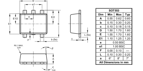
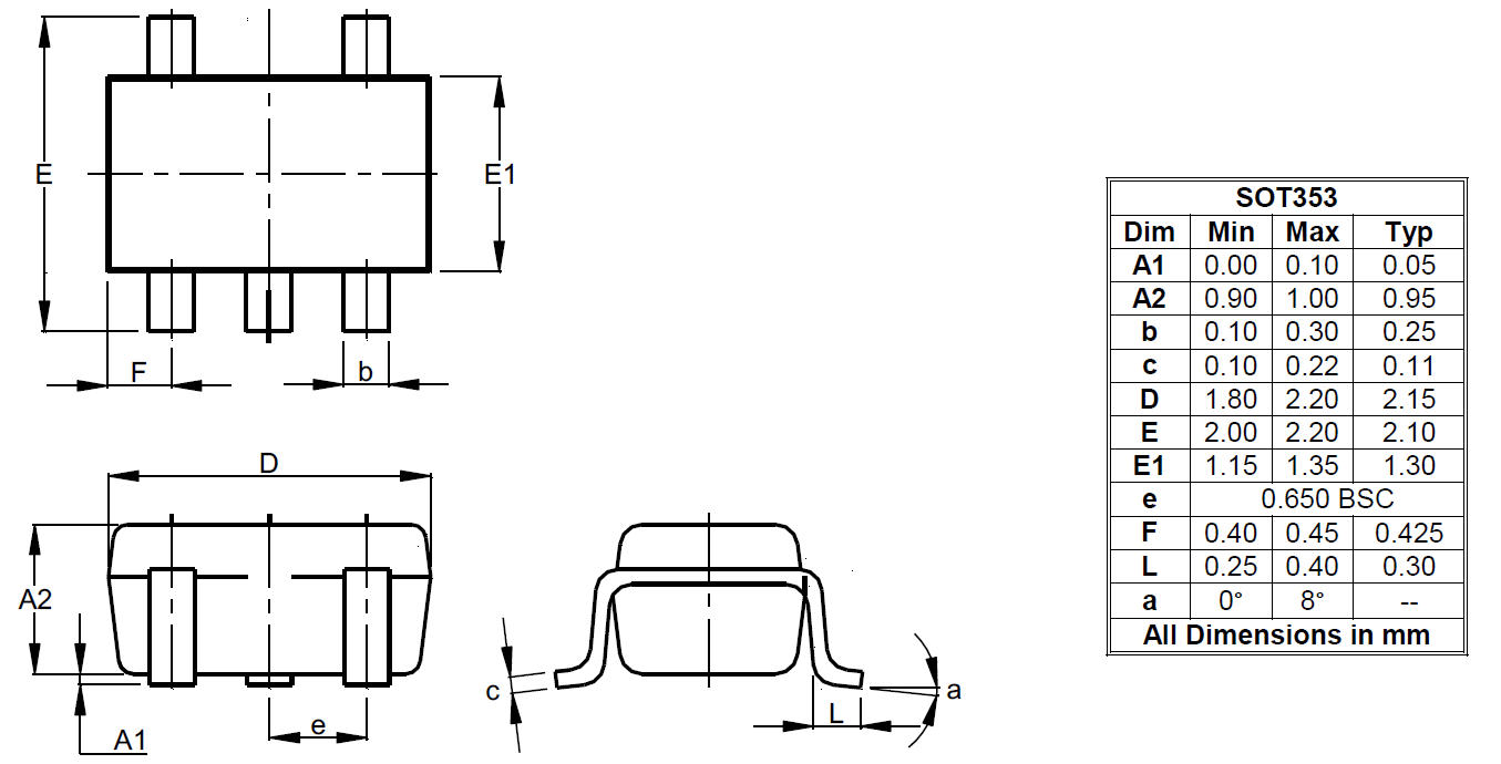
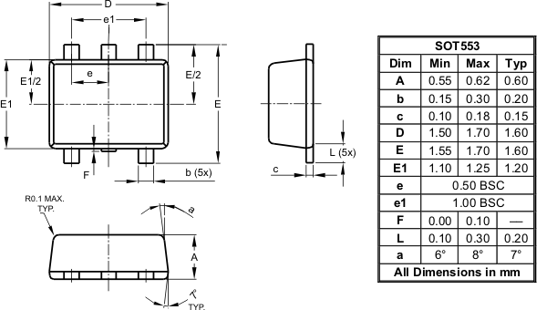
Image shown is for reference only. Actual package may vary. Refer to the product data sheet for package details. SOT25
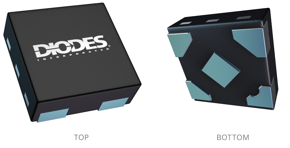
Image shown is for reference only. Actual package may vary. Refer to the product data sheet for package details. X2-DFN0808-4
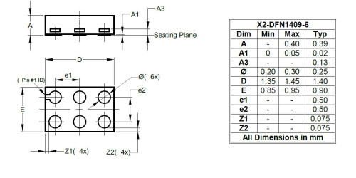
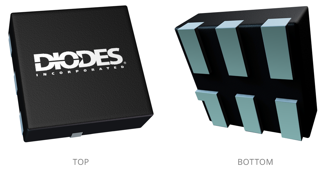
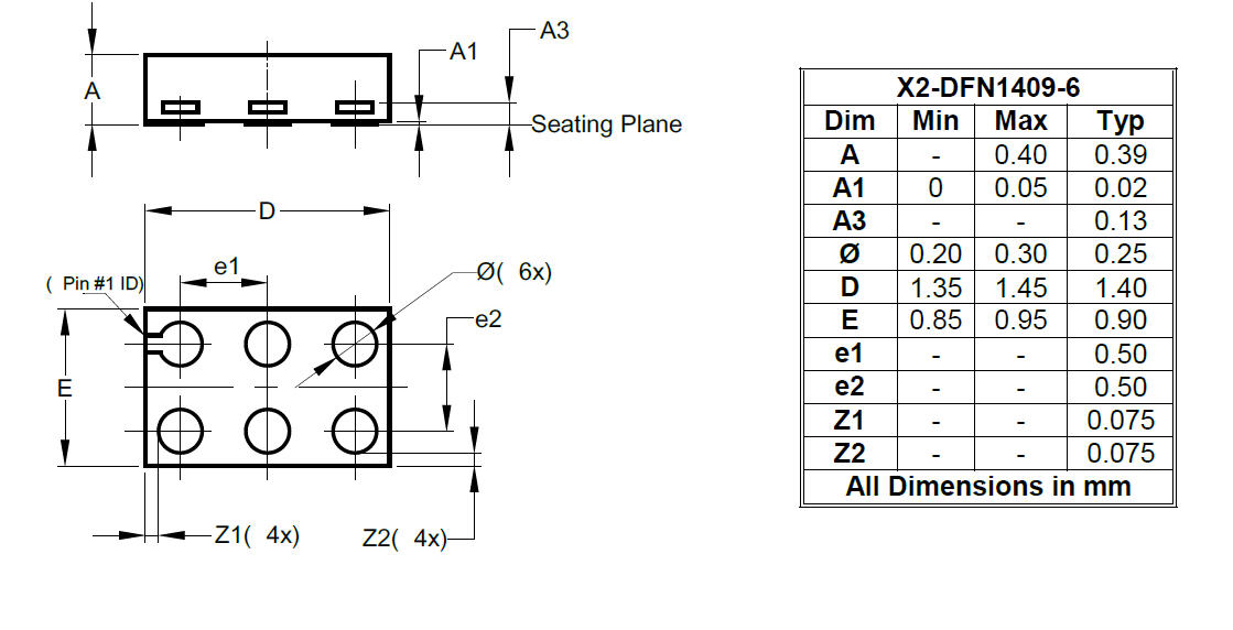
Image shown is for reference only. Actual package may vary. Refer to the product data sheet for package details. X2-DFN1010-6
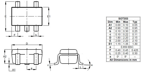
Image shown is for reference only. Actual package may vary. Refer to the product data sheet for package details. X2-DFN1410-6
Image shown is for reference only. Actual package may vary. Refer to the product data sheet for package details. SOT25
Single Buffer, 3-State, OE LOW
Log in or register to manage email notifications about changes to datasheets or PCNs for this part.
The 74LVC1G125 is a single non-inverting buffer/bus driver with a 3-state output. The output enters a high impedance state when a HIGH-level is applied to the output enable (OE) pin. The device is designed for operation with a power supply range of 1.65V to 5.5V. The inputs are tolerant to 5.5V allowing this device to be used in a mixed voltage environment. The device is fully specified for partial power down applications using IOFF. The IOFF circuitry disables the output preventing damaging current backflow when the device is powered down.
| Function | Buffer |
|---|---|
| Type | Buffers/Inverters/Transceivers |
| Compliance (Only Automotive Supports PPAP) | Standard |
| Channels | 1 |
| Family | LVC |
| VCC Min (V) | 1.65 |
| VCC Max (V) | 5.5 |
| Input Type | Standard CMOS |
| Output Type | 3-State |
| Output Current (mA) | 32 |
Something went wrong with your request. Please try again later. If this problem continues, please contact Diodes support for assistance.
