3 Things You Need to Know about USB Switches
Chris A. Ciufo, Editor-in-Chief, Embedded Intel Solutions magazine
If you’re designing with USB 2.0 or 3.0, you need to know these three things about moving USB signals around your system.
Chances are you are now—or soon will be—designing USB into your embedded system. That’s because USB is used everywhere!
It’s tough to forecast how many USB 2.0 (480 Mbps) or USB 3.0 (5 Gbps) channels there are in the world because USB is (nearly) as ubiquitous as LED lights.
But looking at some ultra-mobile devices that contain USB gives some idea just how popular USB is: 317million PCs, 321 million tablets, and 2 billion mobile phones (source: Gartner Device Shipments, July 2014). And every one of Apple’s recently announced ultra-slim MacBook will sport the very latest—and wickedly flexible—Enhanced SuperSpeed USB 3.1 Type-C connector.
So listen up, please. I’m going to tell you three things you need to know about USB switches—the digital MUXes and crossbars that fanout USB signals as part of most embedded designs. We’ll stick to USB 2.0 and 3.0 since they make up the bulk of the market.
1. USB Speeds, Pinouts and Switches
A USB switch is basically a MUX/De-MUX that bi-directionally moves USB signals between multiple ports and maintains adherence to USB-IF specifications. The most common switch configuration is a 2:1, although other configurations are possible such as Pericom Semiconductor’s PI2USB4122 4:1.
While USB 1.1 and 2.0 are relatively low speed, the 5 GHz frequency of USB 3.0 presents some signal integrity challenges, as we’ll see later (Table1).
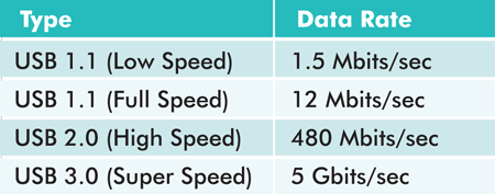
Table 1: USB switches are used extensively for USB 2.0/3.0 channels, and designers should be concerned about signal integrity (SI) with 3.0’s speed.
USB 2.0 has four pins, while USB has nine (Tables 2 and 3). The common, large USB Standard A connector is the end inserted into a USB hub, looks similar for USB 2.0 and 3.0, but is labeled “SS” (Super Speed) for 3.0 and is backwards compatible into USB 2.0 slots. The four backwardly compatible USB 2.0 pins are cleverly integrated into the upgraded seven pin 3.0 Standard A connector. Switches used for USB 3.0 are backward-compatible with USB 2.0 signals, but not vice versa.

Table 2: USB 2.0 pin and signal names. (Courtesy: Diodes Incorporated.)
One footnote, lest you ask. We’re confining our discussion to signal switches as opposed to protocol switches. The former are concerned mostly with the electrical physical layer (PHY) of the OSI model. Protocol switches also exist—and our sponsor Pericom Semiconductor makes a ton of them—but they deal with additional layers of the stack and can interface to more than just USB; for example, they can also switch PCI Express and USB. Let’s keep it simple for now in this short primer.
Table 3: USB 3.0 pin and signal names. USB 3.0 is full duplex and differential. (Courtesy: Diodes Incorporated.)
2. Key Switch Parameters
The basis for a USB switch is an NMOS transistor that’s suitable for hot-swap/plug applications and fast switching. Adding a charge pump widens the rail-to-rail output voltage and allows a higher Vdd operating range while still maintaining moderate ~250μA power consumption (Figure 1). Besides the fanout of the switch, there are a number of key parameters that characterize them.

Figure 1: A charge pump-enhanced NMOS transistor is at the root of USB signal switches.
Maximize 3dB bandwidth: A common industry convention is to measure the max signal frequency of a channel at the 3dB loss point. This is trivial for USB 2.0 at 480 Mbps, but significant for USB 3.0’s 5 Gbps. A good target for a USB 3.0 switch should be >2.5 Gbps. Vendors like Pericom Semiconductor boast up to 10.6 GHz for their best switches.
Lowest insertion loss: It’s desirable to minimize the power loss caused by the switch at operating frequency. Greater than ~-0.8 dB attenuation will lower signal peaks and slow rise/fall times; all of these degrade signals and could result in violating the USB 3.0 spec.
Lowest return loss: A measure of the impedance mismatch between signal and switch, with a design goal to maximize power transfer. Alternatively, this is the ratio of the power into the switch versus reflected power (in dB) where a higher absolute number is better. By convention, the reciprocal is used: the reflected power over incident power (in dB). For example, Pericom’s PI3USB302-A USB 3.0 2:1 switch has a return loss of -23.3 dB at 2.5 GHz.
Minimal crosstalk: Crosstalk describes the extent that signals affect each other through the switch through capacitive, inductive, or conductive coupling. Lower crosstalk numbers are better. Pericom switches routinely boast -33dB but can be as “clean” as -41dB at 2.5 GHz.
On resistance (Ron) and Ron flatness: These are bit more esoteric, where Ron is the resistance through the closed switch—specifically between the transistor source and drain (Figure 1). Like return loss, it should be minimal for maximum power transfer. Ron flatness merely charts the difference between the max and min resistance over the full signal range.
Off isolation: related to crosstalk, off isolation describes the amount of noise in an “off” state switch picked up by an adjacent switch in an “on” state. Since analog signals (digital signals in the real world are analog) become noisier at higher frequency, it’s important in USB 3.0 switches that “off” isolation is high. For example, Pericom’s PI2USB4122 4:1 signal switch has an “off” isolation of -23dB at 3 GHz.
Bit-to-skew and channel-to-channel skew: are measures of how the signal low-to-high and high-to-low transitions for each bit vary per cycle and between channels on multi-channel switches. The target is a symmetric rise/fall waveform which, according to Pericom, doesn’t eat into the timing budget for a signal integrity “eye” opening.
ESD protection and overvoltage: The ability to withstand ESD and overvoltage is critical with USB, since cables are exposed to consumers. +2kV human body model (HBM) is the minimum for ESD; values that are 2x or 4x better (up to +8kV) provide better protection. Designers can improve these values using external shunts, but that adds cost and real estate.
Overvoltage protection describes the ability to short USB signals to Vcc without local damage and without sending the short to downstream devices. Overvoltage is important because consumer-grade cables, plus repetitive plug/unplug cycles, wear the connectors and/or fray the cables and cause shorts. This is a particular problem for cheap cables without strain relief at high stress points.
3. Example Applications
Many CPUs, MCUs and peripherals include only a single USB 2.0 or 3.0 channel. A switch is like a “Y” adaptor, turning one USB 2.0 or 3.0 port into two, four or more, while maintaining good electrical characteristics and high signal integrity. But what are some examples of their use?
USB 2.0 with debug: Figure 2 shows a slick use of a 2:1 USB 2.0 signal switch used to debug a system where the D+/D- pins can be “regular” USB 2.0 signals or a proprietary UART interface. If a USB device instructs the MCU first that it should look for debug signals on its UART pins, the MCU can tell the switch to change ports and energize the port connected to the UART.

Figure 2: USB 2.0 switch in a debug application. (Courtesy: Diodes Incorporated.)
Note that this same 2:1 set-up can also apply in reverse; that is, sharing a single USB 2.0 port (such as on a PC/104 single board computer) with two external peripherals. In Figure 3, the internal flash memory has a USB interface, while WiFi storage is a proprietary interface.

Figure 3: Sharing dissimilar external peripherals. In this case, a USB Flash drive and WiFi storage share a single USB port—such as on an embedded PC/104 board or Arduino UNO HDK. (Courtesy: Diodes Incorporated)
Notebook docking or SBC transition module: Figure 4 shows a classic notebook docking station application where a single USB 3.0 computer port fans out to two additional ones. Shown is Pericom’s PI3USB3102 2:1 USB 3.0/2.0 signal switch. Because the upstream port is USB 3.0 the 9-pin SuperSpeed connector is used, but USB 2.0 signals are present.

Figure 4: USB 3.0 switch in a notebook docking application.